Fuse for use in a semiconductor device, and semiconductor devices including the fuse

Inactive Publication Date: 2005-04-12
MICRON TECH INC
View PDF40 Cites 32 Cited by
  • Summary
  • Abstract
  • Description
  • Claims
  • Application Information

AI Technical Summary

Benefits of technology

Preferably, the narrowed region is disposed adjacent the interface between a second well of the two separate wells and the common well. Accordingly, as a programming current is applied to the fuse, the fuse will preferably become discontinuous adjacent the interface between the second well and the common well. Thus, a first remaining portion of the fuse will lie adjacent a first well of the two separate wells and the region of the n-well adjacent thereto, while a second portion of the discontinuous fuse will lie adjacent only the second well of the two separate wells. After the fuse has been blown, as current is applied to the fuse, the current will pass into the first of the two separate wells and, thus, into the common well through the first portion of the “blown” fuse. A diode, which exists at the interface between the second well of the two separate wells and the common well, which interface is also referred to as a p-n junction, as a depletion zone, as a boundary, or as a border, prevents electrical current from entering the second of the two separate wells through the common well. Accordingly, as the fuse is open, “blown,” or otherwise becomes discontinuous at the narrowed region thereof, the fuse will no longer conduct a significant amount of current and, therefore, an open circuit is created.
Since the fuse material comprises metal suicide, the fuse of the present invention inhibits reconnection of the fuse by growth of a metal silicide layer and, therefore, re-closing of the circuit is prevented.

Problems solved by technology

One disadvantage of ROM devices is that their programming is permanently determined during fabrication and cannot, therefore, be changed.
As the fuse melts, the metal or polysilicon of the fuse “blows” or becomes discontinuous, breaking the conductive link across the fuse.
The use of lasers to “blow” fuses has, however, become increasingly difficult as the size of the features of semiconductor devices, including the fuses thereof, decreases and as the density of features of semiconductor devices increases.
As the programming current or laser beam intensity required to “blow” a conventional fuse may damage regions or structures of the semiconductor device proximate the fuse, conventional fuses are somewhat undesirable.
Moreover, if the use of laser beams is desired to program the fuses of a semiconductor device, the fuse pitch and, thus, the density of structures on the semiconductor device may be limited.
This is especially problematic when such a fuse is disposed adjacent a region, such as an n-well, of a semiconductor substrate conductively doped to have a first conductivity type to bridge two separate conductive wells, such as p-wells, of a second conductivity type, opposite the first conductivity type, disposed adjacent the region of first conductivity type.
Thus, a fuse that blows in such a manner may undesirably conduct current having substantially the same characteristics as current conducted across an intact fuse.
The “blown” fuse may thus undesirably conduct current having substantially the same characteristics as current conducted across an intact fuse.

Method used


Image

  • Fuse for use in a semiconductor device, and semiconductor devices including the fuse
  • Fuse for use in a semiconductor device, and semiconductor devices including the fuse
  • Fuse for use in a semiconductor device, and semiconductor devices including the fuse

Examples


Embodiment Construction

The following description provides specific details about the fuse and methods of the present invention in order to provide a thorough understanding of the present invention. The skilled artisan, however, would understand that the present invention may be practiced without employing these specific details. Indeed, the present invention can be practiced in conjunction with other materials, differently configured structures, and other fabrication techniques, such as those known in the industry.

The process steps and structures described herein do not form a complete process flow for fabricating semiconductor devices or a completed device. Only the process steps and structures necessary to understand the present invention are described.

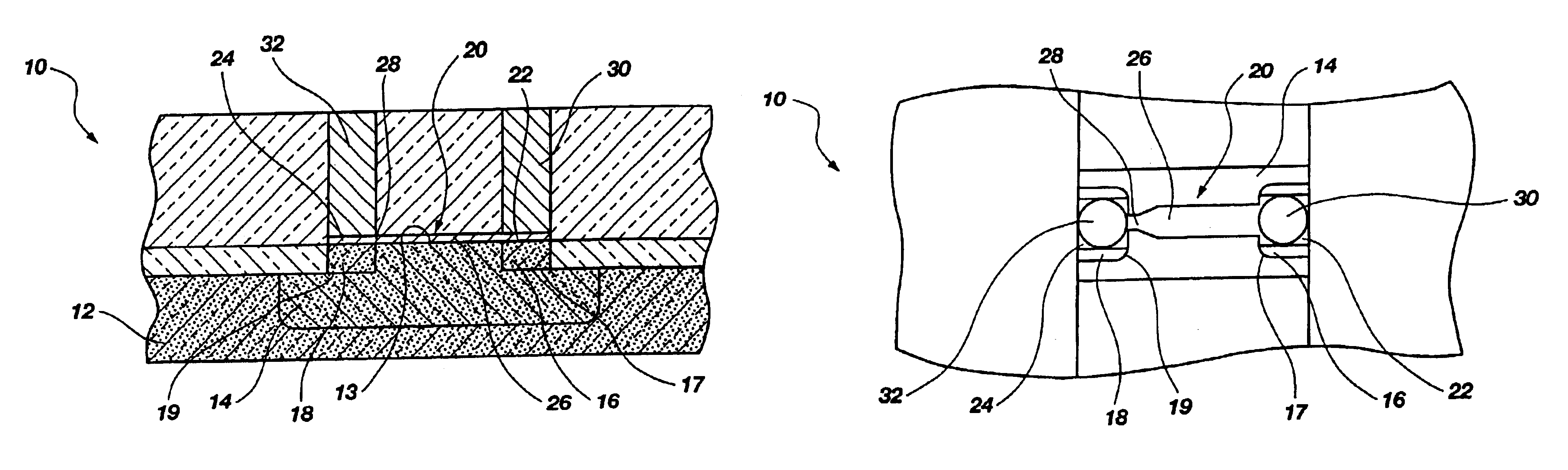
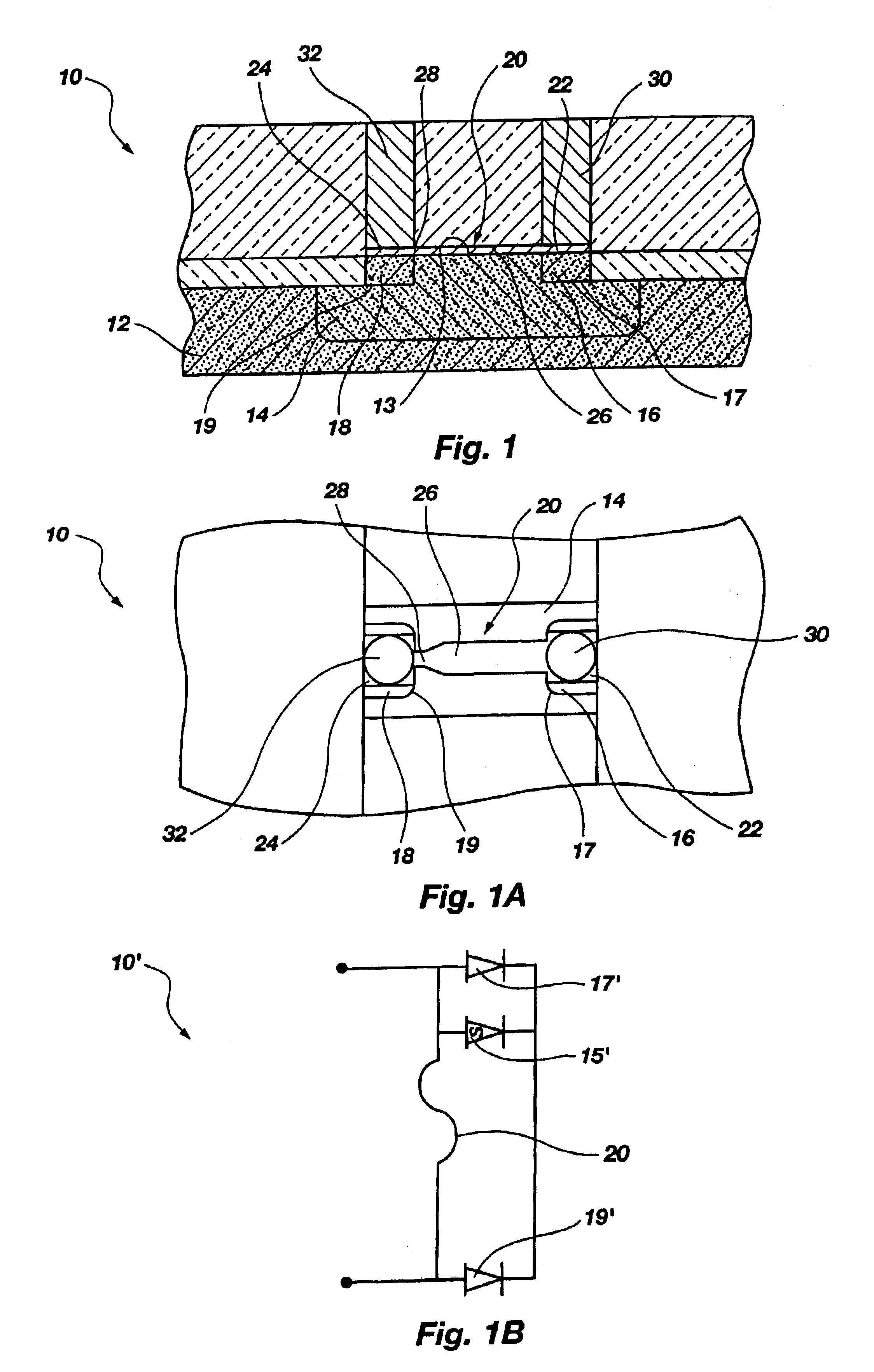
With reference to FIGS. 1 and 1A, a semiconductor device 10 including a fuse 20 according to the present invention is illustrated. Semiconductor device 10 includes a semiconductor substrate 12 within which a common well 14 of a first conductivity type is ...


PUM


Abstract

A metal silicide fuse for a semiconductor device. The fuse includes a conductive region positioned adjacent a common well of a first conductivity type, a terminal region positioned adjacent a well of a second conductivity type, and a narrowed region located between the terminal region and the conductive region and positioned adjacent a boundary between the two wells. Upon applying at least a programming current to the fuse, the fuse “blows” at the narrowed region. The diode or diodes between wells of different conductivity types wells and the Schottky diode or diodes between the remaining portions of the fuse and wells adjacent thereto control the flow of current through the remainder of the fuse and through the associated wells of the semiconductor device. When the fuse has been “blown,” the diodes and Schottky diodes prevent current of a normal operating voltage from flowing through the wells of the semiconductor device.

Description

BACKGROUND OF THE INVENTION1. Field of the InventionThe present invention generally relates to the design and fabrication of semiconductor devices. Specifically, the present invention relates to a fuse for use in a semiconductor device, to methods of fabricating the fuse, and to a semiconductor device that includes the fuse. In particular, the present invention relates to a silicide fuse of a semiconductor device and to a semiconductor memory device that includes the silicide fuse. More particularly, the present invention relates to a semiconductor device that includes two diffusion regions disposed substantially within a well of opposite conductivity type, each of which communicates with an end of a metal silicide fuse.2. Background of Related ArtComputers typically include devices that store data, such as memory devices. A first type of memory device is referred to as a read only memory (“ROM”) device, in which data is permanently stored and cannot be overwritten or otherwise alte...

Claims


Application Information

Patent Timeline
IPC IPC(8): H01L23/525H01L23/52
CPCH01L23/5256H01L2924/0002H01L2924/00
Inventor MARR, KENNETH W.VIOLETTE, MICHAEL P.
Owner MICRON TECH INC
Why Eureka
Try Eureka