Method of manufacturing a semiconductor device to provide a plurality of test element groups (TEGs) in a scribe region

Inactive Publication Date: 2005-04-19
RENESAS ELECTRONICS CORP
View PDF12 Cites 39 Cited by
  • Summary
  • Abstract
  • Description
  • Claims
  • Application Information

AI Technical Summary

Benefits of technology

[0024]According to the foregoing methods, a number of TEGs can be arranged in the scribe region, and the large amount of data can be obtained by evaluating the characteristic of the TEGs. Therefore, it becomes possible to maintain and improve the yield of a semiconductor product in the development and the mass production thereof.
[0025]The characteristic evaluation or the failure analysis of an actual device can be performed by cont

Problems solved by technology

On the other hand, many patterns necessary for a manufacturing process of, for example, a phototarget and an alignment mark are included in the scribe region, and thus the number of the TEGs to be disposed therein is limit

Method used


Image

  • Method of manufacturing a semiconductor device to provide a plurality of test element groups (TEGs) in a scribe region
  • Method of manufacturing a semiconductor device to provide a plurality of test element groups (TEGs) in a scribe region
  • Method of manufacturing a semiconductor device to provide a plurality of test element groups (TEGs) in a scribe region

Examples


Example

(First Embodiment)

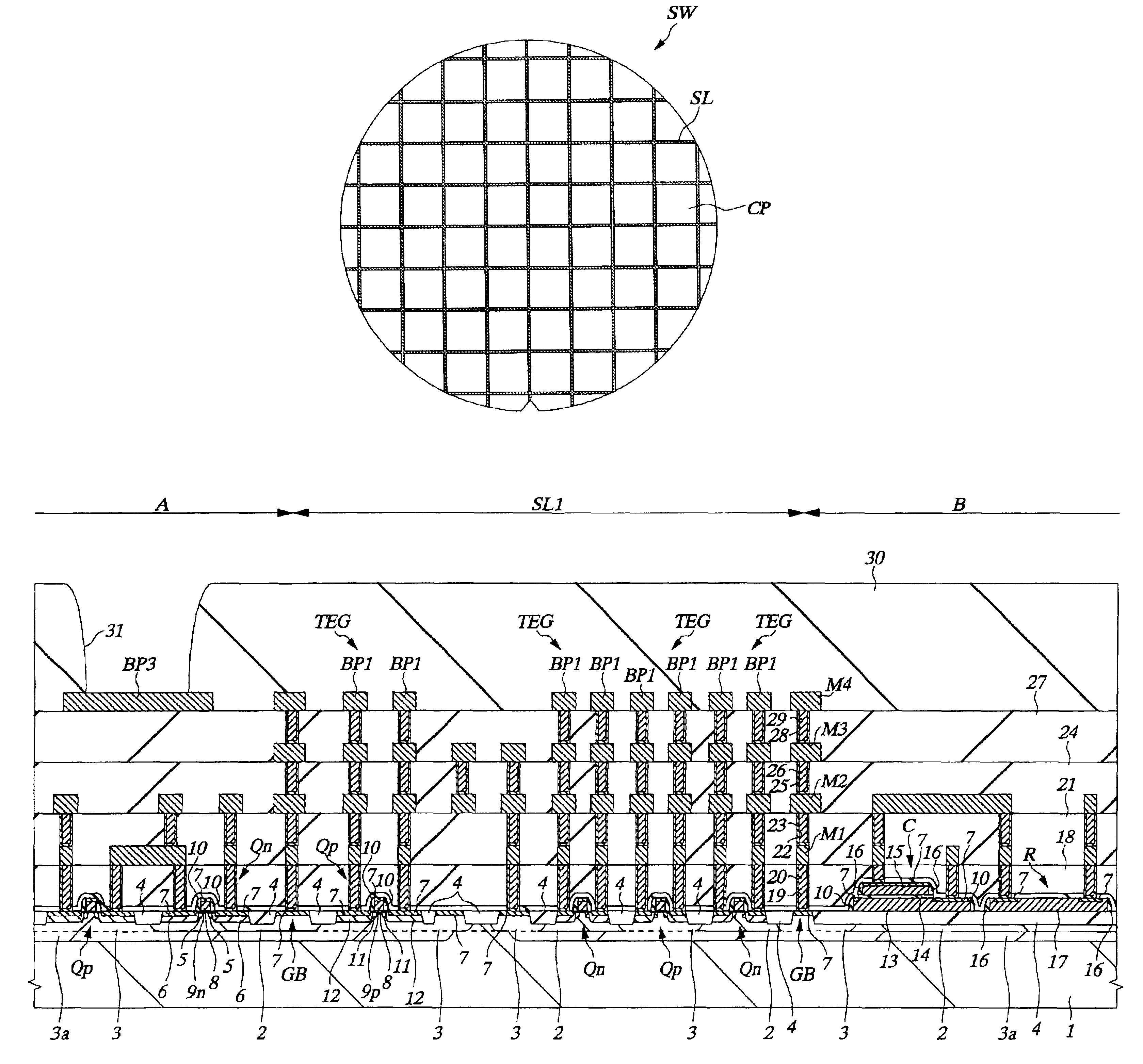
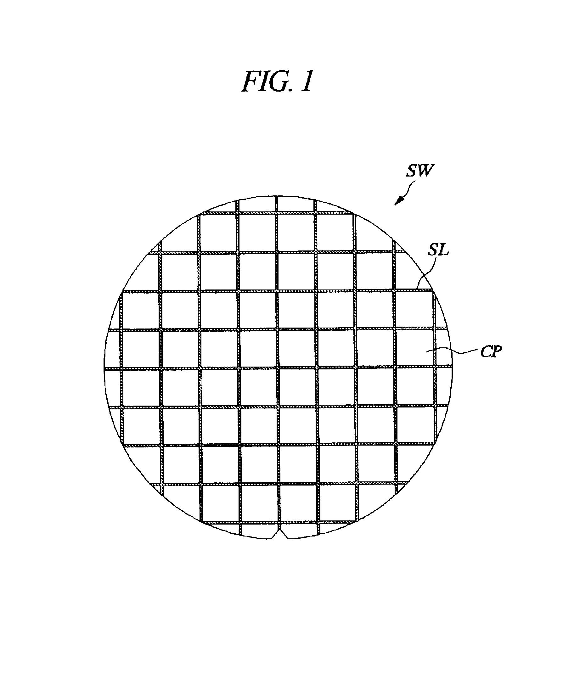
[0078]FIG. 1 shows a scribe region SL on a wafer SW.

[0079]A chip CP on which a semiconductor integrated circuit is manufactured is not created separately one by one, but several tens of or hundreds of them are simultaneously manufactured together on one wafer SW, and then the wafer is divided into each of the chips CP. A step for dividing the wafer SW into each of the chips CP is called a dicing or a scribing, in which the wafer SW is completely cut by a circular cutting blade having a width of about 50 μm and rotating at a high speed. The region used in the abovementioned cutting is a scribe region (represented by a half-tone dot meshing in FIG. 1), which has a width of, for example, about 100 μm.

[0080]Guard bands functioning to prevent the water from permeating into the semiconductor integrated circuit are formed around the semiconductor integrated circuit, and the region sandwiched between the adjacent guard bands can be taken as a scribe region SL. As described...

Example

(Second Embodiment)

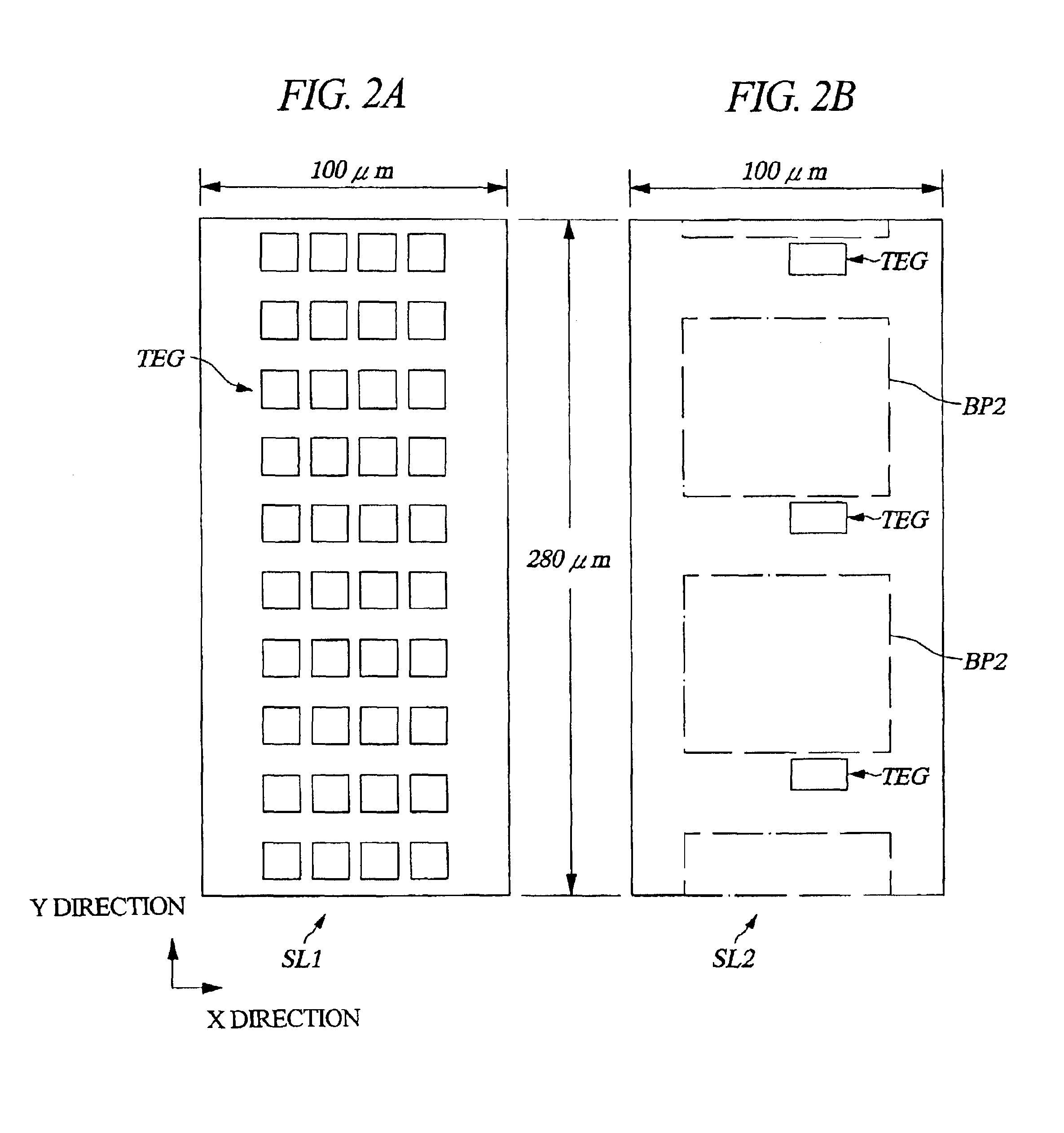
[0152]In the foregoing first embodiment, descriptions have been made for the TEG provided with the first electrode pad BP1 which is a rectangular electrode having a side length of 0.5 μm or shorter and the TEG provided with the second electrode pad BP2 which is a rectangular electrode having a side length of 20 μm or longer. In this second embodiment, however, descriptions will be made for a TEG provided with both of the first electrode pad BP1, which is a rectangular electrode having a side length of 0.5 μm or shorter, and the second electrode pad BP2, which is a rectangular electrode having a side length of 20 μm or longer.

[0153]FIG. 19 is a plan view showing an example of the principal part of a plurality of TEGs and electrode pads arranged in a third scribe region SL3.

[0154]The TEG constituted of the MISFET is shown in the third scribe region SL3 as an example. The first electrode pad BP1 (represented by a half-tone dot meshing in FIG. 19) is a minute rectangu...

Example

(Third Embodiment)

[0160]Descriptions will be made for the characteristic evaluation or the failure analysis of an actual device of a semiconductor product using a nanoprobe according to the third embodiment. A CMOS inverter circuit that is one of the basic logic circuits shown in FIG. 22 is exemplified as the actual device, and the measuring method of a logic value thereof will be described. FIG. 22A is a circuit diagram of a CMOS inverter circuit, and FIG. 22B is a perspective view showing the principal part of a semiconductor substrate illustrating an n channel MISFET Qn and a p channel MISFET Qp constituting the CMOS inverter circuit. In FIG. 22B, an example where a nanoprobe is contacted to an extraction electrode constituted of a first wiring layer is shown. In the case of a multi-layered wiring, however, the nanoprobe can be contacted to an extraction electrode constituted of the uppermost layer wiring of the two or more wiring layer. In FIG. 22B, the reference symbol SUB deno...


PUM


Abstract

Disclosed is a technique capable of improving a yield of a semiconductor device by measuring a plurality of TEGs arranged in a scribe region. A first electrode pad connected to each terminal of a TEG is formed as a rectangular, minute, isolated pattern having a side length of about 0.5 μm or shorter and constituted of an uppermost layer wiring on a semiconductor substrate, and therefore, a great number of TEGs can be laid in a first scribe region. The characteristic evaluation or the failure analysis is performed by contacting a nanoprobe having a tip radius of curvature of 0.05 μm to 0.8 μm to the first electrode pad.

Description

TECHNICAL FIELD OF THE INVENTION[0001]The present invention relates to a semiconductor device and a technique for manufacturing the same. Particularly, the present invention relates to a technique effectively applicable to a semiconductor device having a semiconductor element used in a characteristic evaluation or a failure analysis.BACKGROUND OF THE INVENTION[0002]The conventional characteristic evaluation or the failure analysis of a semiconductor element has been performed using an apparatus, for example, prober, in which a needle called a probe is contacted to an electrode formed on a surface of a test element group (hereinafter, referred to as TEG), and then an electrical contact to a specific portion of the semiconductor element is measured.[0003]Some methods have been proposed to determine measurements using the prober. For example, in Japanese Patent Application Laid-Open No. 9-326425, by S. Tomimatsu et al., a method is disclosed in which a plurality of probes each having a...

Claims


Application Information

Patent Timeline
IPC IPC(8): H01L23/544G01R31/28H01L21/28H01L21/3205H01L21/66H01L21/822H01L23/52H01L27/04
CPCH01L22/34H01L2924/3011H01L2924/0002H01L2924/00
Inventor ASAYAMA, KYOICHIROMITSUI, YASUHIROARAKAWA, FUMIKOKAMOHARA, SHIROOHJI, YUZURU
Owner RENESAS ELECTRONICS CORP
Why Eureka
Try Eureka