High-speed data buffer

a buffer and high-speed technology, applied in the field of high-speed data buffers, can solve problems such as errors in sampling data, certain amount of error data, and problems for high-speed circuit designers

Inactive Publication Date: 2005-04-19
VIA TECH INC
View PDF10 Cites 10 Cited by
  • Summary
  • Abstract
  • Description
  • Claims
  • Application Information

AI Technical Summary

Benefits of technology

[0011]In order to overcome the above problem, it is the primary object of the present invention to provide a high-speed data buffer, wherein a buffer circuit is divided into two sampling circuits composed of a rising-edge device and a falling-edge device by using double data rate sampling technique adopting both the rising edge and the falling edge of the clock signal. In such manner, the data buffer of the present invention can be applicable to a single data rate buffer adopting either the rising edge or the falling edge of the clock signal and also a double data rate buffer adopting both the rising edge and the falling edge of the clock signal. Moreover, the timing margin of the flag signal can be prolonged from half a clock cycle to a full clock cycle so as to meet the requirement for high-speed applications.

Problems solved by technology

In recent years, as the demands for a higher speed of data processing and a higher frequency for operation in the computer system continuously increase, designers of high-speed circuits have often encountered problems due to insufficient processing timing margin.
Therefore, the receiving end meets a serious problem in that insufficient timing leads to an error when the data are input into the data buffer.
When the transitions of the first flag signal FLAG1 and the second flag signal FLAG2 occur during clock III, the excess pulse (labeled as “b”) may cause a certain amount of error data input into the buffer such that the incomplete pulse (labeled as “c”) may lead to an error of sampling data.
In such a manner, the mentioned insufficient timing problem in that the error data are stored in the buffer occurs and may become more serious in high-speed data transfer operations.
Moreover, in the prior art, the transitions of the flag signals can only be performed in a half-a-clock-cycle low-level region of the timing of the clock signal; otherwise, the excess pulse signal may cause an error storage of the data.

Method used


Image

  • High-speed data buffer
  • High-speed data buffer
  • High-speed data buffer

Examples


Embodiment Construction

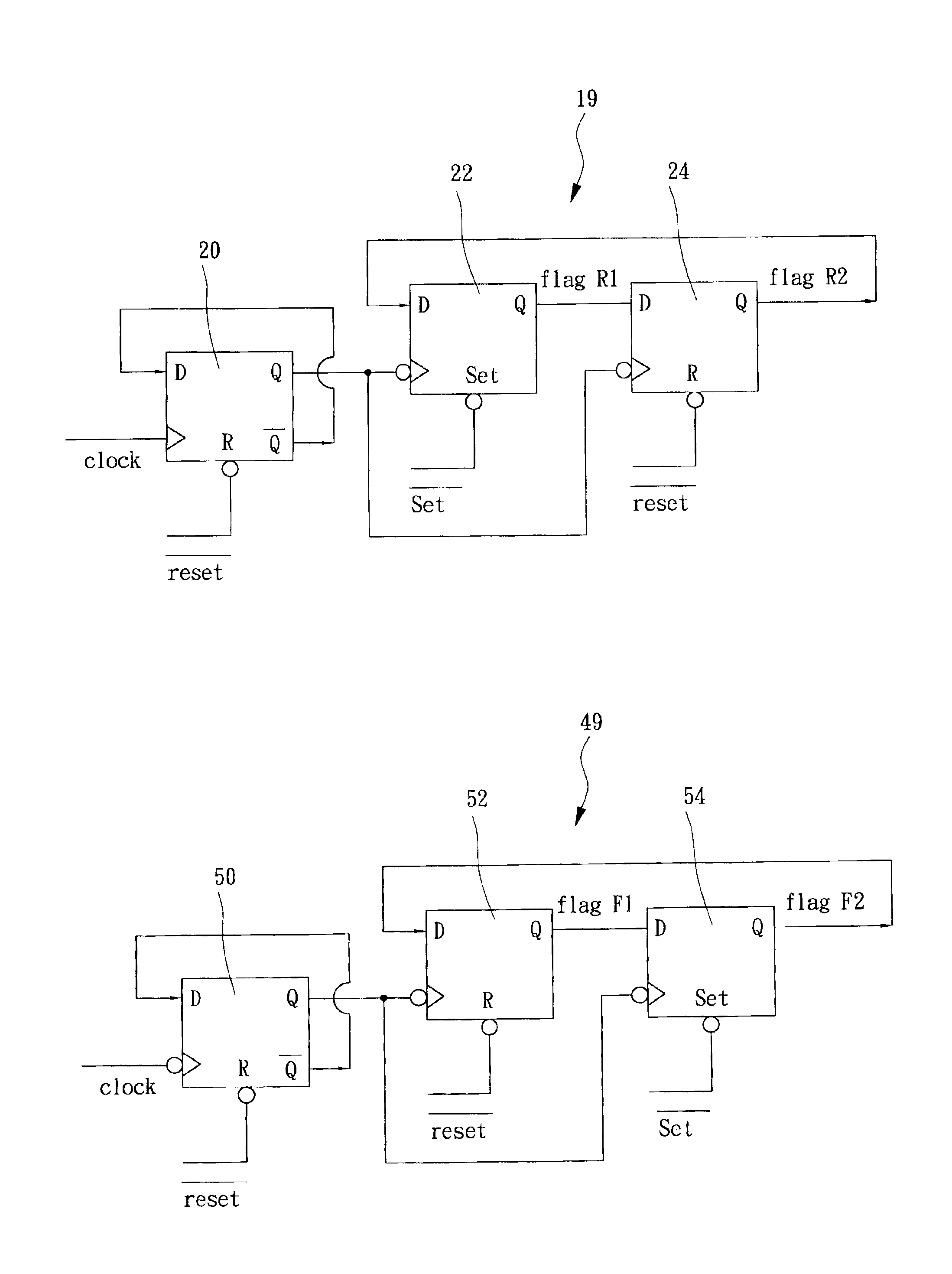
[0033]The present invention provides a high-speed data buffer, wherein a buffer circuit comprising a ring counter is divided into two sampling circuits comprising a rising-edge portion and a falling-edge portion, and AND gates and OR gates are used for generation of sampling clock signals. In such a manner, the excess pulse edge can be ensured to occur before the correct edge so that the error data caused by the excess pulse can be over-written with the correct data input afterwards. Therefore, a clock cycle of timing margin can be obtained and-the data stored in the data buffer can be ensured to be correct.

[0034]For a further explanation of the present invention, to begin with, the rising-edge device comprises a trigger circuit and a plurality of rising-edge circuits so as to store the data. For the trigger circuit, please refer to FIG. 6, which is a circuit diagram illustrating a trigger circuit 19 (ring counter) of the rising-edge portion in accordance with one embodiment of the ...


PUM


Abstract

Disclosed is a high-speed data buffer, wherein a buffer circuit composed of a ring counter is divided into two sampling circuits composed of a rising-edge portion and a falling-edge portion, and both of the two sampling circuits comprises a trigger circuit and a sampling clock generation circuit. In such a manner, the excess pulse edge can be ensured to occur before the correct edge so that the error data caused by the excess pulse can be over-written with the correct data input afterwards. Therefore, a clock cycle of timing margin can be obtained and the data stored in the data buffer can be ensured to be correct.

Description

BACKGROUND OF THE INVENTION[0001]1. Field of the Invention[0002]The present invention generally relates to a high-speed data buffer, and more particularly, to a data buffer applicable to a single data rate buffer adopting either the rising edge or the falling edge of the clock signal and also a double data rate buffer adopting both the rising edge and the falling edge of the clock signal. Such a high-speed data buffer is suitable for use in high-speed data communication systems.[0003]2. Description of the Prior Art[0004]In recent years, as the demands for a higher speed of data processing and a higher frequency for operation in the computer system continuously increase, designers of high-speed circuits have often encountered problems due to insufficient processing timing margin. Therefore, it has become an important topic to well control the timing of the rising edge and the falling edge of the clock signal.[0005]On the other hand, IEEE-1394 has become a standard for communication i...

Claims


Application Information

Patent Timeline
Patent Type & Authority Patents(United States)
IPC IPC(8): G06F5/06H04L7/02
CPCH04L7/02G06F5/06
Inventor GAU, SHYH-PYNG
Owner VIA TECH INC
Why Eureka
Try Eureka