Optical amplifier

a technology of optical amplifier and optical signal, which is applied in the direction of electromagnetic repeaters, instruments, and active medium materials, can solve the problems of loss portion, noise figure deterioration, and loss ratio of optical signal of l band compared to optical signal of c band, and achieve the effect of reducing the relative optical sn ratio of one wavelength band and simple construction

Inactive Publication Date: 2005-04-19
FUJITSU LTD
View PDF29 Cites 42 Cited by
  • Summary
  • Abstract
  • Description
  • Claims
  • Application Information

AI Technical Summary

Benefits of technology

[0012]The present invention focuses on the above points, with a first object of providing an optical amplifier for performing amplification of optical signals of two wavelength bands, wherein deterioration in the relative optical SN ratio for one wavelength band is reduced. Moreover, a second object is to provide an optical amplifier of a simple construction which can deal with restrictions on installation space, power consumption and the like. Furthermore, a third object is to provide an optical amplifier enabling the balance control of the optical power with respect to respective wavelength bands is possible.
[0014]With such a construction, the optical signals of the second wavelength band can be Raman amplified, by employing a part of the excitation light used in the optical amplifying device. Hence the optical signals of the second wavelength band which have been Raman amplified are amplified by the optical amplifying device. As a result, the optical SN ratio for the second wavelength band is improved, and optical signals with uniform characteristics in the respective wavelength bands can be obtained.
[0018]With such a construction, in the pre-stage optical amplifying device provided at the input stage, the optical signals of the first wavelength band are amplified to a sufficient level, while for the optical signals of the second wavelength band, the insufficient gain portion is amplified by the post-stage optical amplifying device. As a result, the construction can be simplified compared to the conventional optical amplifier.
[0020]With such a construction, balance control of the optical power of the first wavelength band and the second wavelength band is performed. As a result, the optical amplification for the respective wavelength bands can be more stably performed. Moreover, it is possible to flexibly correspond to changes in the channels being used.

Problems solved by technology

However, since the demultiplexer is provided on the input side of the respective C band and the L band optical amplifying sections, there is a problem that the noise figure deteriorates by the insertion loss portion.
However, with the above mentioned C / L band optical amplifier, there is the drawback in that there are many cases where the noise figure for the C band optical amplifying section and the noise figure for the L band optical amplifying section are different, so that in general, the optical SN ratio for the optical signal of the L band deteriorates compared to that for the optical signal of the C band.
As a result, the power consumption of the overall optical amplifier increases.
In particular, in the case where, as with optical amplifiers used for example as undersea repeaters or the like, there are restrictions from the view point of installation space, power consumption or other factors, it is difficult to realize a construction such as shown in FIG.

Method used


Image

  • Optical amplifier
  • Optical amplifier
  • Optical amplifier

Examples


first embodiment

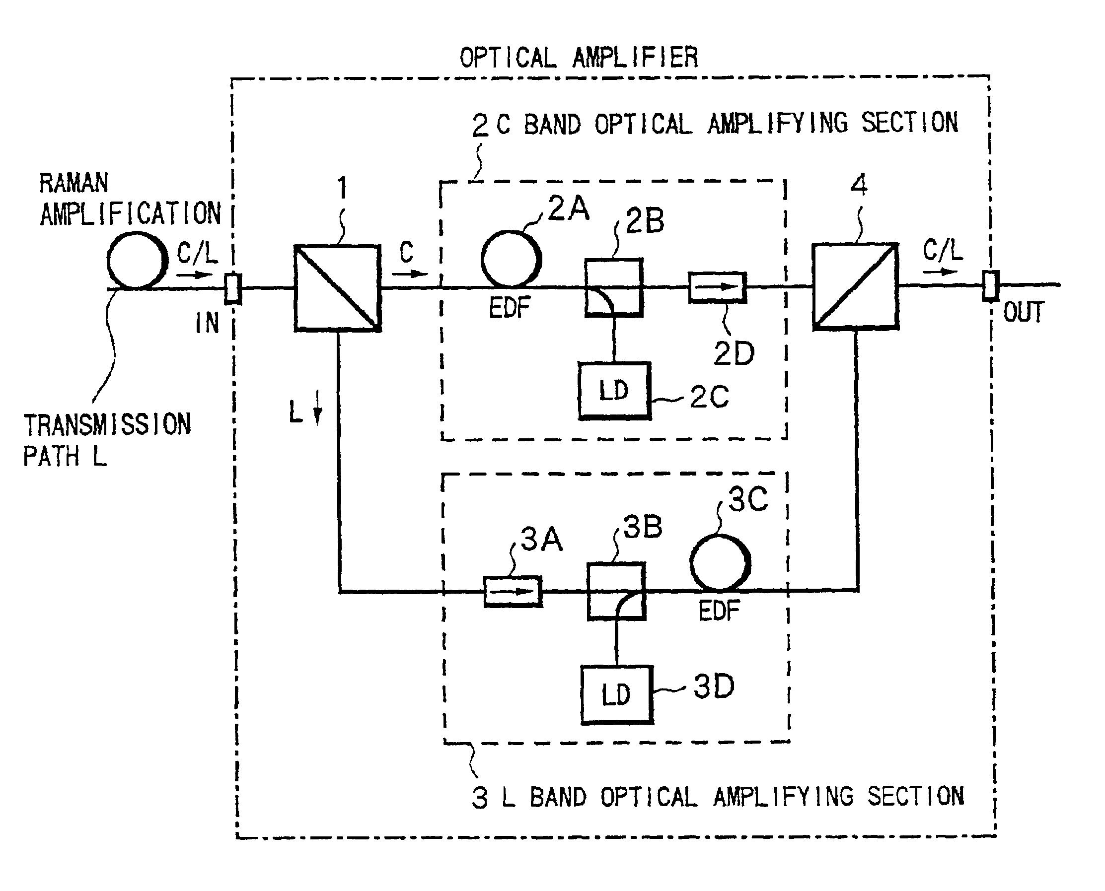
[0048]FIG. 1 is a block diagram showing a basic construction of an optical amplifier according to a

[0049]In FIG. 1, the present optical amplifier has a demultiplexer 1 serving as a demultiplexing device for demultiplexing WDM signal light input from an external transmission path L via a terminal IN, into a C band optical signal and an L band optical signal, a C band optical amplifying section 2 serving as a first optical amplifying section for amplifying the C band optical signals which have been demultiplexed by the demultiplexer 1, an L band optical amplifying section 3 serving as a second optical amplifying section for amplifying the L band optical signals which have been demultiplexed by the demultiplexer 1, and a multiplexer 4 serving as a multiplexing device for multiplexing optical signals which have been respectively amplified by the C band optical amplifying section 2 and the L band optical amplifying section 3, and outputting these to the outside via a terminal OUT.

[0050]H...

second embodiment

[0071]Next is a description of the present invention.

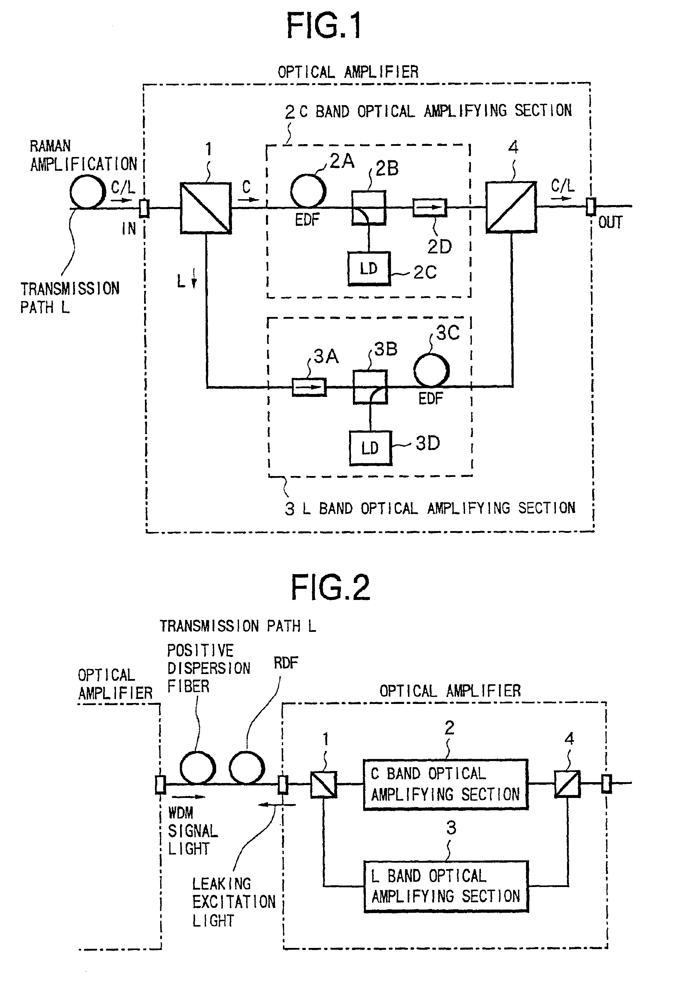
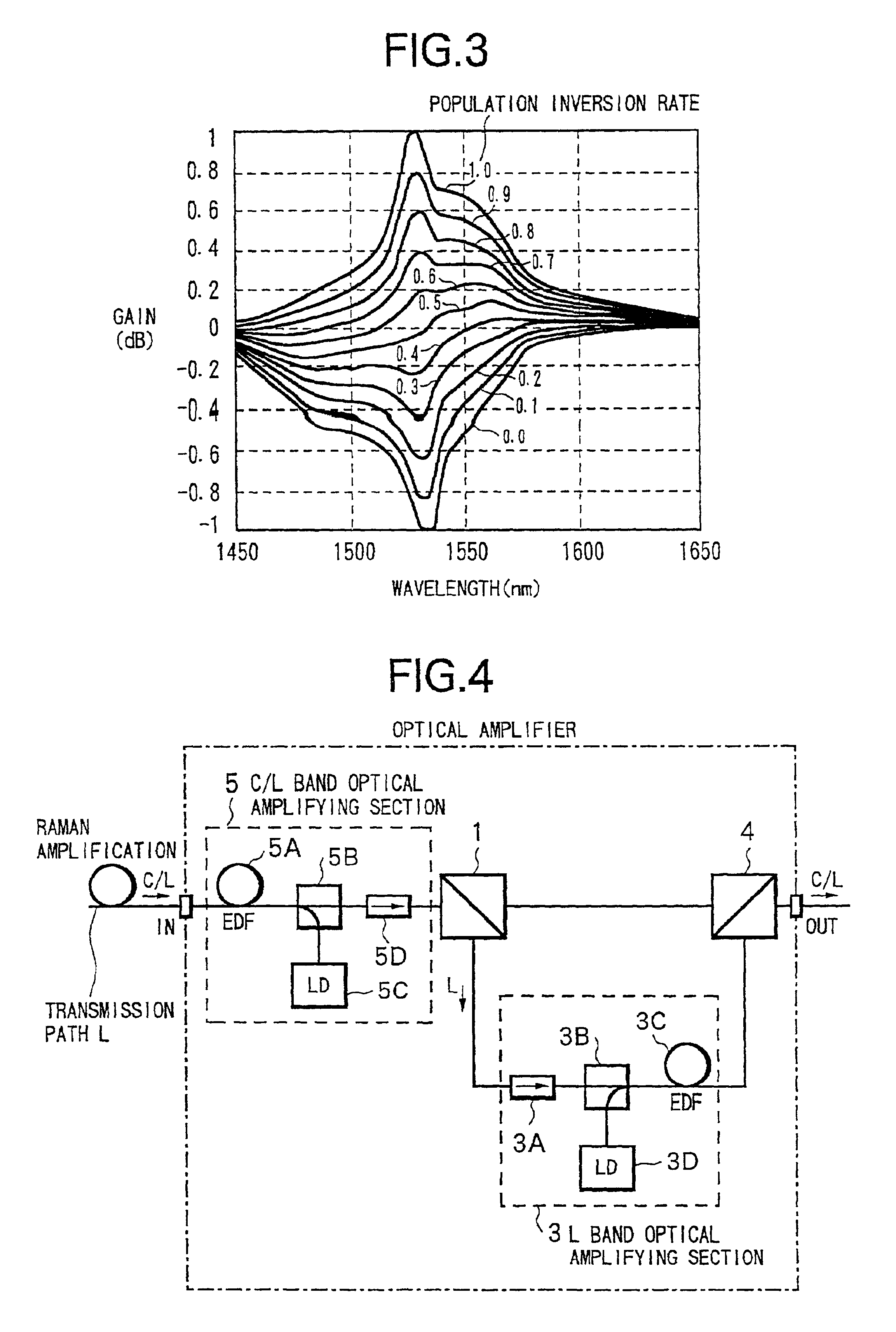
[0072]FIG. 4 is a diagram showing a basic construction of an optical amplifier according to the second embodiment Parts of the same construction as for the first embodiment are denoted by the same reference numerals. The same applies for the subsequent figures.

[0073]In FIG. 4, the optical amplifier has a C / L band optical amplifying section 5 as a pre-stage amplification section for amplifying WDM signal light input from an external transmission path L via a terminal IN, a demultiplexer 1 for demultiplexing optical signals which have been amplified by the C / L band optical amplifying section 5 into a C band optical signal and an L band optical signal, an L band optical amplifying section 3 for amplifying L band optical signals which have been demultiplexed by the demultiplexer 1, and a multiplexer 4 for multiplexing the C band optical signals which have been demultiplexed by the demultiplexer 1, and the L band optical signals which ...

third embodiment

[0081]Next is a description of the present invention.

[0082]With the third embodiment, the case is considered where for example in the second embodiment described above, compensation for the wavelength dispersion and dispersion slope, or compensation for the gain wavelength characteristics can be executed inside the optical amplifier.

[0083]FIG. 5 shows a structural example of an optical amplifier according to the third embodiment.

[0084]In FIG. 5, the construction of the present optical amplifier is such that compensation optical devices 6C and 6L are respectively provided on the light transmission paths corresponding to the respective bands, between the demultiplexer 1 and the multiplexer 4. Here, the compensation optical device 6C corresponding to the C band is inserted between the demultiplexer 1 and the multiplexer 4, while the compensating optical device 6L corresponding to the L band is inserted between the L band optical amplifying section 3 and the multiplexer 4. The insertion...


PUM

PropertyMeasurementUnit
wavelengthaaaaaaaaaa

Abstract

An optical amplifier is provided for performing amplification of optical signals of two wavelength bands, where deterioration in the optical SN ratio relative to one wavelength band is reduced, with a simple construction which can deal with restrictions on installation space, power consumption and the like. To this end, the present optical amplifier has a C / L band optical amplifying section for amplifying respective optical signals of a C band and an L band, a demultiplexer for demultiplexing output light from the C / L band optical amplifying section into the C band and the L band, an L band optical amplifying section for amplifying L band optical signals which have been demultiplexed by the demultiplexer, and a multiplexer for multiplexing the C band optical signals which have been demultiplexed by the demultiplexer and the L band optical signals which have been amplified by the L band optical amplifying section. The construction is such that a part of excitation light of a 1480 nm band used in the C / L band optical amplifying section is supplied via an input terminal to a Raman amplification producing medium of a transmission path, and Raman amplified L band optical signals are input to the C / L band optical amplifying section.

Description

BACKGROUND OF THE INVENTION[0001](1) Field of the Invention[0002]The present invention relates to an optical amplifier for amplifying wavelength division multiplexed signal light. In particular the invention relates to an optical amplifier for collectively amplifying wavelength division multiplexed signal light which includes optical signals of two wavelength bands.[0003](2) Description of the Related Art[0004]With conventional long distance light transmission systems, light transmission is performed using light regeneration repeaters which convert optical signals into electric signals to effect re-timing, re-shaping, and regenerating. However recently, with progress in the utilization of optical amplifiers, optical amplifier repeater transmission systems which use optical amplifiers as linear repeaters are being investigated. By replacing a light regeneration repeater with an optical amplifier repeater, the number of parts in the repeater can be greatly reduced, with the prospect o...

Claims


Application Information

Patent Timeline
Patent Type & Authority Patents(United States)
IPC IPC(8): H01S3/06H04B10/17H01S3/067H01S3/30H01S3/16H01S3/094H01S3/23G02F1/35H01S3/10H04B10/07H04B10/2525H04B10/29H04B10/296H04J14/00H04J14/02
CPCH01S3/06758H04B10/2916H04B10/2931H01S3/094042H01S3/1608H01S3/2375H04B2210/258H01S3/302H01S3/2383
Inventor SHIMOJOH, NAOMASANAITO, TAKAO
Owner FUJITSU LTD
Why Eureka
Try Eureka