

Method for manufacturing spacer for electron source apparatus, spacer, and electron source apparatus using spacer
a technology of electron source apparatus and manufacturing method, which is applied in the manufacture of electrode systems, electric discharge tubes/lamps, and tubes with screens, etc., and can solve the problem of hardly occurring heat fusion of substrates
- Summary
- Abstract
- Description
- Claims
- Application Information
AI Technical Summary
Benefits of technology
Problems solved by technology
Method used
Image

Examples
embodiment 1
[0072]Description will now be first given on a method for manufacturing a spacer used in an embodiment 1 and then on a structure and a manufacturing method of a display panel of an image display apparatus using that spacer.
[0073](Embodiment 1)
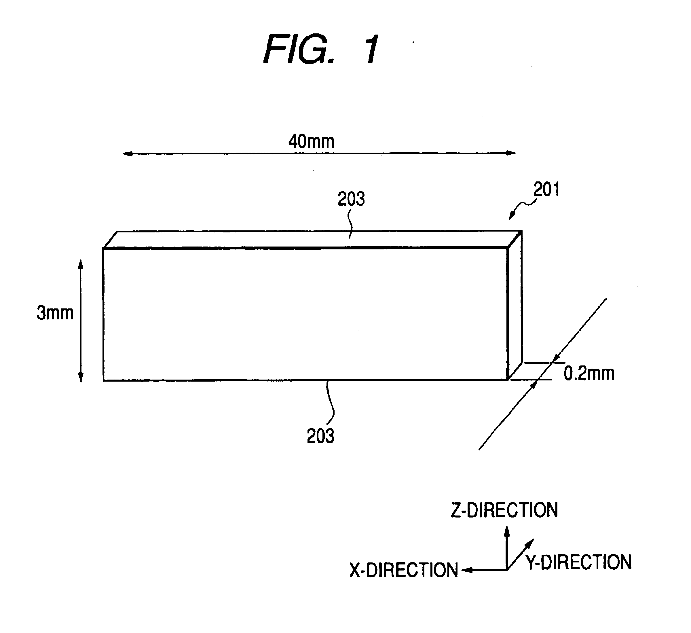
[0074]The spacer used in the embodiment 1 is manufactured in the following manner. As shown in FIG. 1, soda lime glass having a 40 mm×3 mm thin sheet rectangular shape with a thickness of 0.2 mm is used as a spacer substrate 201. 3 mm corresponds to a thickness of the display panel. In this embodiment, the spacer substrate is manufactured by cutting the soda lime plate glass having a thickness of 0.2 mm. The present invention is not restricted to cut of the plate glass, and the glass may be processed into a desired shape by, for example, a heating drawing method. Further, X, Y and Z directions are determined as shown in FIG. 1.
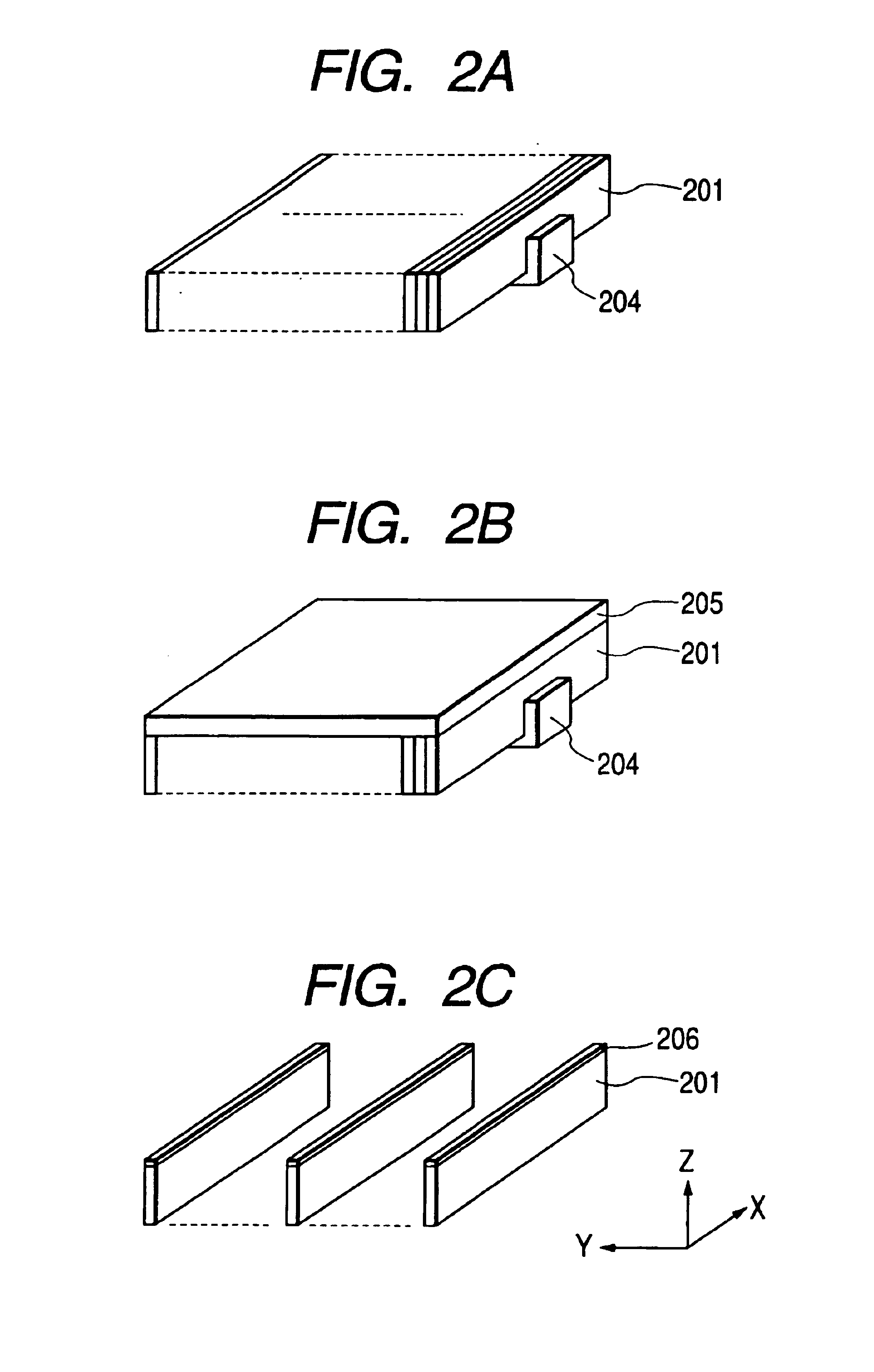
[0075]A conductive film is then formed on a desired position on the spacer substrate.
[0076]The conductive film is forme...
embodiment 2
[0126](Embodiment 2)
[0127]The spacer used in the embodiment 2 is produced as follows. Each reference numeral corresponds to each part in the embodiment 1.
[0128]In this embodiment, an alumina substrate is used as the spacer substrate 201. Its dimension is the same as that in the embodiment 1.
[0129]The conductive film 206 is then formed at a desired position (equal to that in the embodiment 1) on the spacer substrate 201.
[0130]As a preparation for formation of the conductive film, the film type material 205 is first produced. Its procedure is described as follows.[0131](1) The SnO2 fine particles and ethylcellulose as the binder are dissolved in turpentine oil which is a solvent;[0132](2) this liquid solution is applied on an appropriate substrate (polytetrafluoroethylene substrate in this embodiment) by the screen printing method;[0133](3) it is dried in an oven at 120° C. for 10 minutes; and[0134](4) it is removed from the polytetrafluoroethylene substrate.
[0135]With this procedure,...
embodiment 3
[0144](Embodiment 3)
[0145]A spacer used in an embodiment 3 is produced as described below. Each reference numeral denotes each corresponding part in the embodiments 1 and 2.
[0146]A soda lime glass substrate (see FIG. 1) similar to that in the embodiment 1 is used as the spacer substrate 210, and a film type material 205 manufactured by the procedure similar to that in the embodiment 1 is used as a material of the conductive film 206.
[0147]The conductive film 206 is then formed at a desired position (equal to the embodiment 1) of the spacer substrate 201.
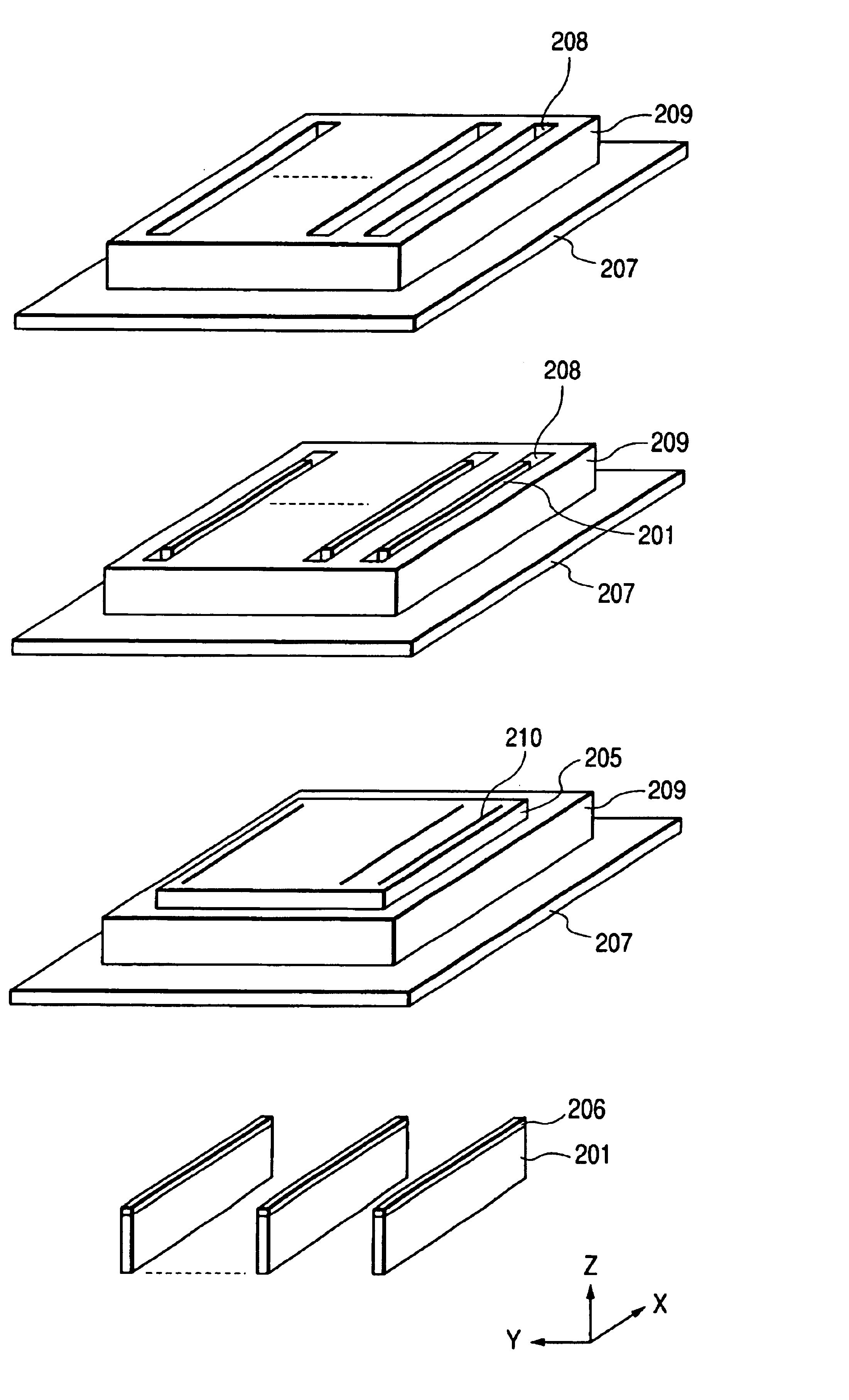
[0148]Its procedure is explained with reference to FIGS. 3A to 3D.[0149](1) A holding jig 209 having holes 208 whose size is substantially the same as that of the spacer is mounted on a horizontal plate 207 (polytetrafluoroethylene substrate in this example) (FIG. 3A);[0150](2) the spacer substrate 201 is set in each hole 208 (FIG. 3B);[0151](3) the film type material 205 is mounted thereon (FIG. 3C);[0152](4) a YAG laser beam is irr...
PUM
 Abstract
Description
Claims
Application Information