Delay optimization in signal routing

Inactive Publication Date: 2005-04-26
XILINX INC
View PDF19 Cites 30 Cited by
  • Summary
  • Abstract
  • Description
  • Claims
  • Application Information

AI Technical Summary

Benefits of technology

[0037]After the router completes the load balancing algorithm, the router attempts to preserve the delay improvements by protecting results just generated. The router identifies all routing resources committed during load balancing optimization and makes it expensive for the

Problems solved by technology

Connection delays have become a significant part of the total delay for transistor-connected devices.
Even for hard-wired ASIC devices, as feature size has become smaller, wiring has begun to contribute a major part to total delay of signals.
Therefore routing can significantly affect timing of the configured logic device.
It becomes difficult to complete later connections legally, e.g., without crossing other signals.
Later connections tend to become longer and less efficient, or produce more shorts t

Method used


Image

  • Delay optimization in signal routing
  • Delay optimization in signal routing
  • Delay optimization in signal routing

Examples


Embodiment Construction

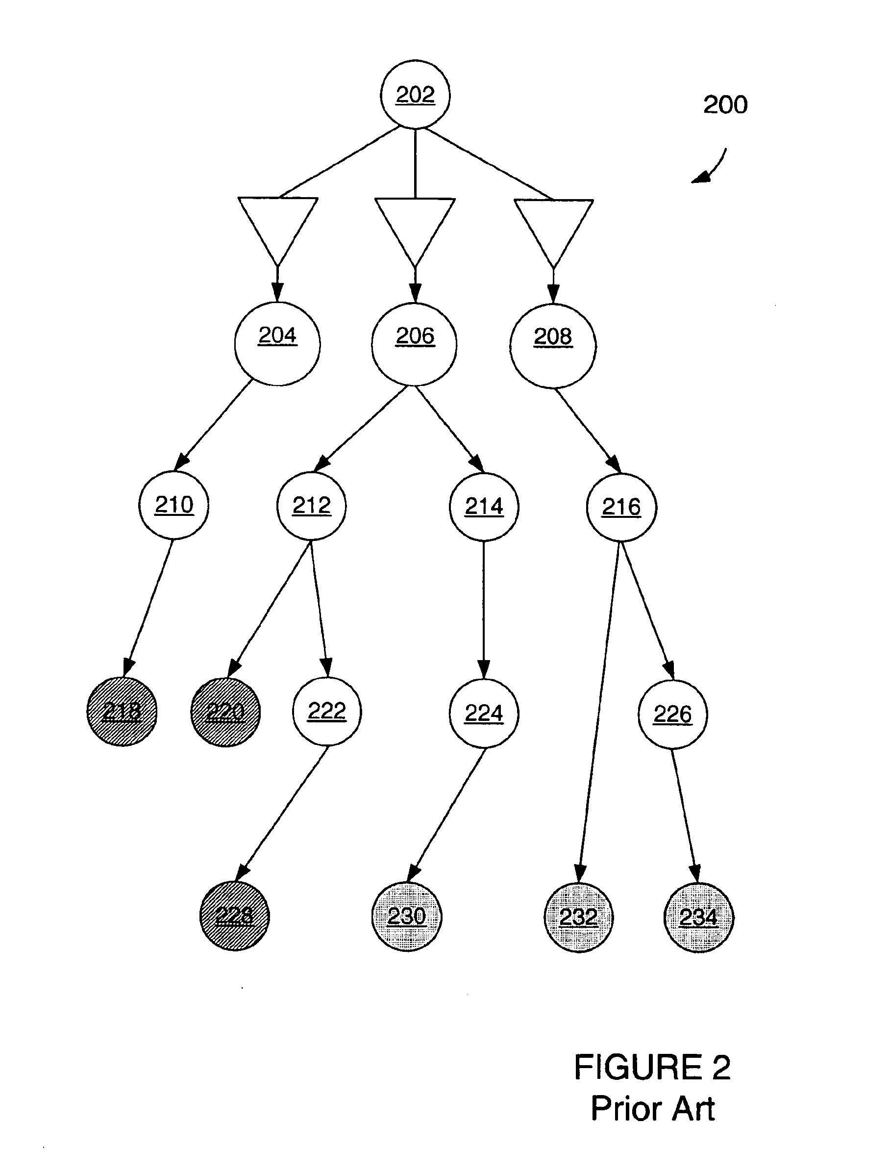
[0046]FIG. 2 schematically illustrates a routing solution 200 of the prior art. The routing solution is represented by a directed graph such that each node (circle) in the graph represents an electrically equivalent wire segment and each arc (line or line plus buffer) in the graph corresponds to a PIP. The arc direction corresponds to the direction of current flow. As shown in FIG. 2, both timing-critical loads, schematically represented by nodes 218, 220, and 228; and non-critical loads, schematically represented by nodes 230, 232, and 234, are routed through large buffered nodes 204, 206, and 208, and intermediate nodes 210, 212, 214, 216, 222, 224, and 226. Routing signals through large buffered nodes exposes the driver to multiple large capacitances, resulting in severe delay.

[0047]FIG. 3 and FIG. 4 illustrate the sequential application of a branching penalty and a load balancing heuristic to the signal of FIG. 2.

[0048]The use of buffered nodes involves a tradeoff. A large input...


PUM


Abstract

A delay optimization algorithm has four major steps: (1) selecting signal connections to target for delay improvement; (2) unrouting all signals containing those candidate connections; (3) rerouting those signals, using a “load-balancing”heuristic; and (4) during rip-up and re-try routing, protecting wiring to all signal loads routed by the heuristic, including non-timing critical loads. Load balancing includes (a) applying a branching penalty on logic cell output wire segments, and (b) encouraging all non-route critical loads to route through a single buffered wire segment.

Description

FIELD OF THE INVENTION[0001]The present invention relates to field programmable gate arrays (FPGAs), and in particular to routing a design so that delays are reduced to meet specified timing requirements.BACKGROUND OF THE INVENTION[0002]Programmable logic devices are available for implementing any of a wide variety of logic designs. The user designs a logic circuit, and uses software to direct a computer to program a logic device to implement the design. Timing of signals passed between parts of the logic device depends in part upon placement of the user's circuit elements into transistor groups in the physical structure and the resultant arrangement of the metal wires. In general, longer wires mean longer delays, the actual timing depending upon capacitances, resistances, and the number of logic elements a signal must traverse. As transistors have become faster, a larger percentage of the delay in passing a signal through the device is contributed by the wiring. Therefore it has be...

Claims


Application Information

Patent Timeline
IPC IPC(8): G06F17/50
CPCG06F17/5077G06F17/5054G06F30/34G06F30/394G06F30/347
Inventor KONG, RAYMOND
Owner XILINX INC
Why Eureka
Try Eureka