Low-power high-performance storage circuitry

a storage circuit and low-power technology, applied in the field of integrated circuits, can solve the problems of affecting battery life, not being able to have devices such as cell phones, personal digital assistants (pdas), palm-top computers, etc., and prolonging battery li

Inactive Publication Date: 2005-05-03
RGT UNIV OF CALIFORNIA
View PDF14 Cites 39 Cited by
  • Summary
  • Abstract
  • Description
  • Claims
  • Application Information

AI Technical Summary

Problems solved by technology

Without high-density memory it would not have been possible to have devices such as cell phones, personal digital assistants (PDAs), palm-top computers, or even laptop computers.
Power Consumption affects battery life, and lower power consumption leads to longer battery life.
Otherwise, rapid depletion of the battery power can limit the use of portable devices and also can inconvenience users of those devices by requiring them to carry spare batteries, for example.
Standby current has several components, and one of the most significant components is due to leakage in memory cells.
Unfortunately, the leakage current in prior memory circuits tended to increase for each generation of technology scaling according to a physical law.
In other words, increased Vt results in both reduced leakage current and increased signal propagation delay within the circuit.
However, lower threshold voltage can result in relatively heavy leakage currents in standby mode.
Unfortunately, there have been reliability problems with this earlier SRAM cell.
Voltage build up at node X-bar can in turn promote more leakage current through m3 potentially causing a transition to a new erroneous locked state.
Thus, current leakage can result in reliability problems by causing erroneous data storage.
Another problem with the prior SRAM structure of FIG. 1A is that the voltage of a cell node can be influenced by bit line voltages during a read operation.
However, increasing the impedance of m6 also slows down the read speed.
Thus, there is a tradeoff between circuit stability and read speed.
Thus, design option “A” would use high Vt to lower the leakage current, but this would cause speed degradation since the signal propagation delay increases as Vt increases for a fixed Vgs (DD) swing.

Method used


Image

  • Low-power high-performance storage circuitry
  • Low-power high-performance storage circuitry
  • Low-power high-performance storage circuitry

Examples


first embodiment

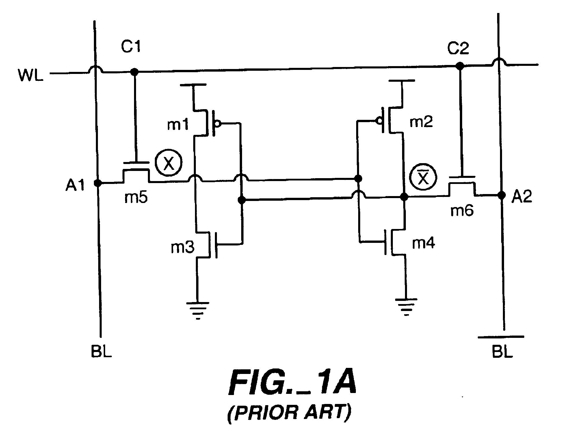
[0043]FIG. 3 is an illustrative circuit diagram of an integrated circuit data storage cell 100 in accordance with the invention. The topology and overall operation of the inventive data storage cell 100 of FIG. 3 is like that of the earlier SRAM cell of FIG. 1A. Transistors shown in FIG. 3 that correspond to transistors of FIG. 1A are labeled with reference numerals that are identical to the reference numerals used in FIG. 1A and that are primed. Therefore, reference can be made to the above description of the prior SRAM cell of FIG. 1A to understand the structure and operation of the new data storage cell of FIG. 3.

[0044]There are important differences between the novel data storage cell 100 of FIG. 3 and the earlier SRAM cell of FIG. 1A. First, the data latching transistors (m1′-m4′) of the novel data storage cell 100 are implemented as high threshold voltage (high Vt) transistors. Second, the access transistors (m5′-m6′) of the novel storage cell 100 are implemented as low thresh...

second embodiment

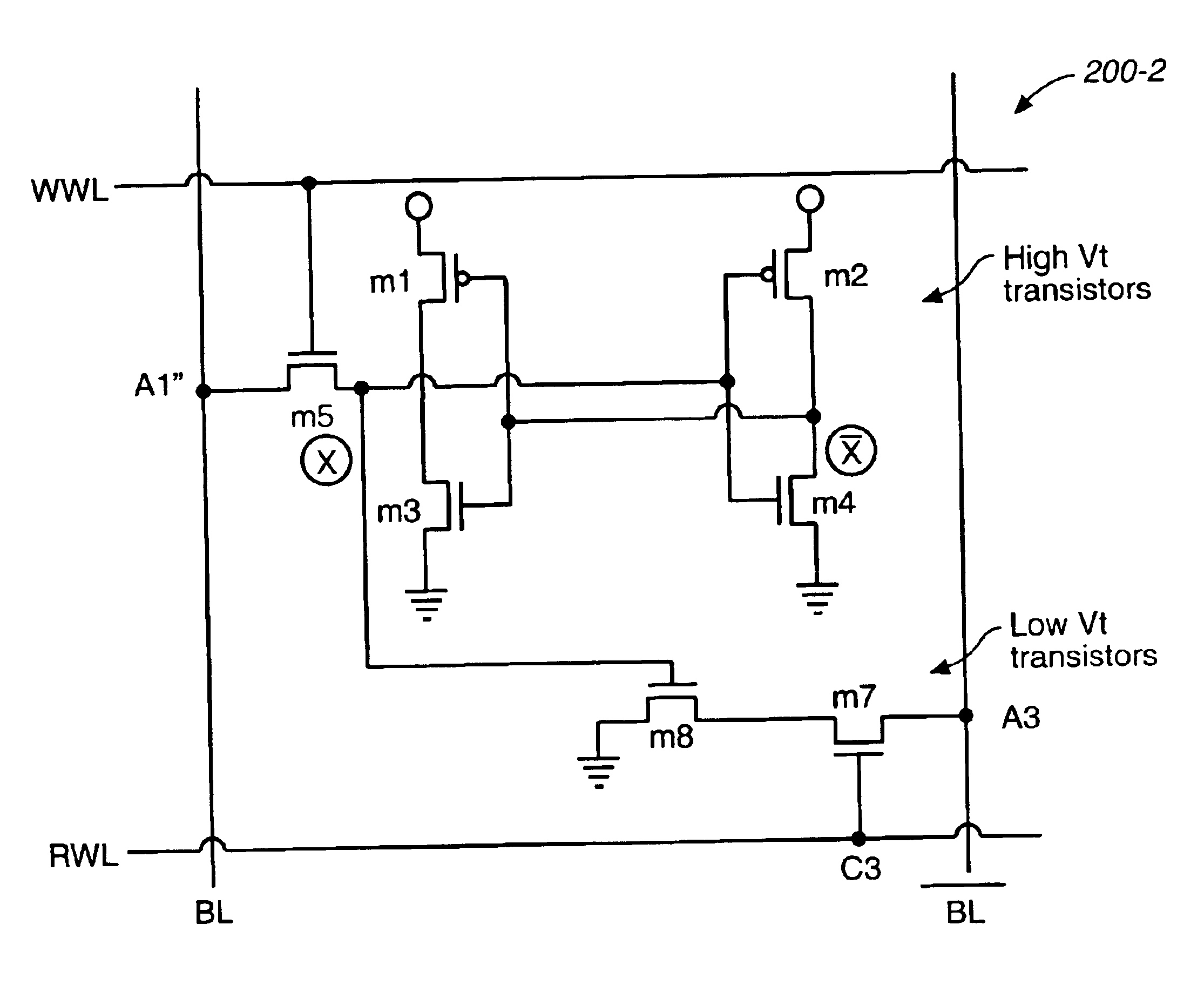
[0045]FIG. 4A is an illustrative circuit diagram of an integrated circuit data storage cell 200 in accordance with the invention. Some portions of the topology and operation of the inventive data storage cell 200 of FIG. 4A are identical to corresponding portions of the novel data storage cell 100 of FIG. 3. Transistors shown in FIG. 4A that correspond to transistors of FIG. 3 are labeled with reference numerals that are identical to the reference numerals used in FIG. 3 and that are double primed.

[0046]The data storage cell 200 includes three sections. A storage circuitry section includes transistors m1″-m4″. A write access circuitry section includes transistors m5″ and m6″. A read access circuitry section includes transistors m7 and m8. Storage transistors m1″-m4″ and write access transistors m5″-m6″ are high Vt transistors. Read access transistors m7-m8 are low Vt transistors. Leakage current is reduced through the use of high Vt transistors in the storage circuitry section and i...

case 3

[0069]Case 3 can be particularly useful in reducing power consumption. For example, when a write word line is enabled, specifically a pulsed write wordline signal is applied, all write transistors are turned on and BL (or BL-bar) is discharged through a write transistor and the cell transistor. For example in FIG. 4A, when X-bar is low, BL-bar is discharged through m6 and m4. The discharged BL-bar should be precharged before the next read operation. The extent of BL-bar discharging depends on the pulse width and the threshold voltage of the write transistor. The larger the pulse width, the larger BL-bar discharging. And the higher the threshold voltage of the write transistor, the smaller BL-bar discharging. When the threshold voltage of the write transistor is high, BL-bar is discharged less due to smaller current driving capability of the transistor. Therefore, a high Vt transistor is used for the write transistor, BL (or BL-bar) is less discharged for the given pulse width, and t...


PUM


Abstract

An integrated circuit is provided comprising a latch circuit including, a first inverter including a first high threshold voltage PMOS transistor and a first high threshold voltage NMOS transistor with a first data node comprising interconnected source / drains (S / D) of the first PMOS and NMOS transistors; a second inverter including a second high threshold voltage PMOS transistor and a second high threshold voltage NMOS transistor with a second data node comprising interconnected source / drains (S / D) of the second PMOS and NMOS transistors; wherein the gates of the first PMOS and first NMOS transistors are coupled to the second data node; wherein the gates of the second PMOS and second NMOS transistors are coupled to the first data node; a first low threshold voltage access transistor including a first S / D coupled to the first data node and to the gate of the second PMOS transistor and to the gate of the second NMOS transistor and including a second S / D coupled to a first data access node and including a gate coupled to a first access control node; and a second low threshold voltage access transistor including a first S / D coupled to the second data node and to the gate of the first PMOS transistor and to the gate of the first NMOS transistor and including a second S / D coupled to a second data access node and including a gate coupled to a second access control node.

Description

CROSS-REFERENCE TO RELATED APPLICATIONS[0001]This application claims priority to and the benefit of the filing date of provisional patent application Ser. No. 60 / 368,392 filed Mar. 27, 2002.BACKGROUND OF THE INVENTION[0002]1. Field of the Invention[0003]The invention relates to integrated circuits, and more particularly, to integrated circuits used in information storage and retrieval.[0004]2. Description of the Related Art[0005]For over three decades the semiconductor industry has been able to take advantage of the technology scaling according to Moore's Law. A continual increase in memory chip density, and thus the on-chip memory capacity has enabled the development of new products such as portable electronic devices used for mobile computing and communications. Without high-density memory it would not have been possible to have devices such as cell phones, personal digital assistants (PDAs), palm-top computers, or even laptop computers. Power Consumption has become a significant ...

Claims


Application Information

Patent Timeline
Patent Type & Authority Patents(United States)
IPC IPC(8): H03K3/012H03K3/356H03K19/00H03K3/00H03K3/3565
CPCG11C11/412H03K19/0016H03K3/356156H03K3/3565H03K3/012G11C2207/2227G11C5/063G11C11/413H03K19/0185
Inventor KANG, SUNG-MOYOO, SEUNG-MOON
Owner RGT UNIV OF CALIFORNIA
Why Eureka
Try Eureka