
Programmable on-chip differential termination impedance

Active Publication Date: 2005-05-03
ALTERA CORP
View PDF56 Cites 21 Cited by
  • Summary
  • Abstract
  • Description
  • Claims
  • Application Information

AI Technical Summary

Problems solved by technology

However, external resistors typically use a substantial amount of board space.

Method used


Image

  • Programmable on-chip differential termination impedance
  • Programmable on-chip differential termination impedance
  • Programmable on-chip differential termination impedance

Examples


first embodiment

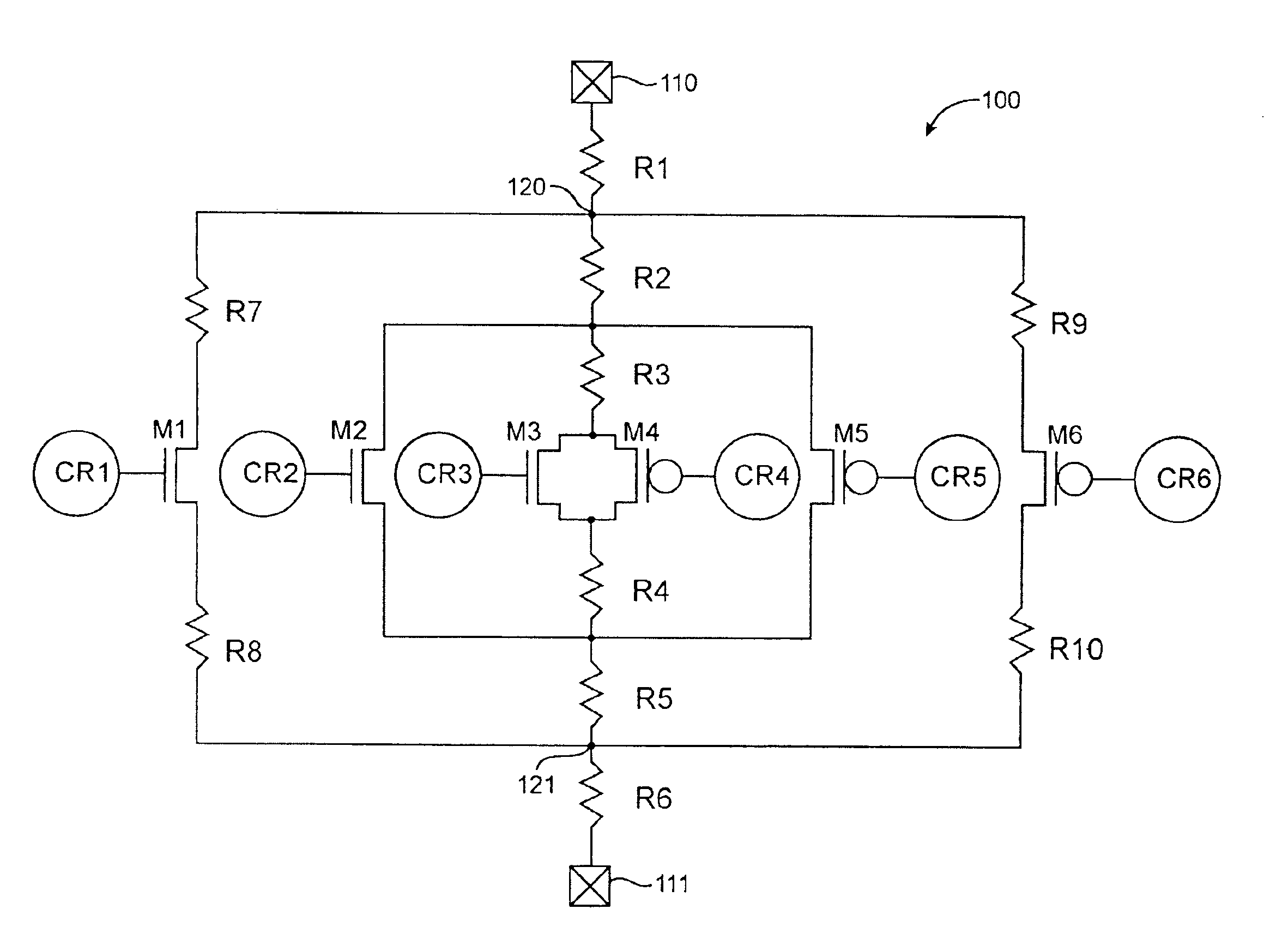
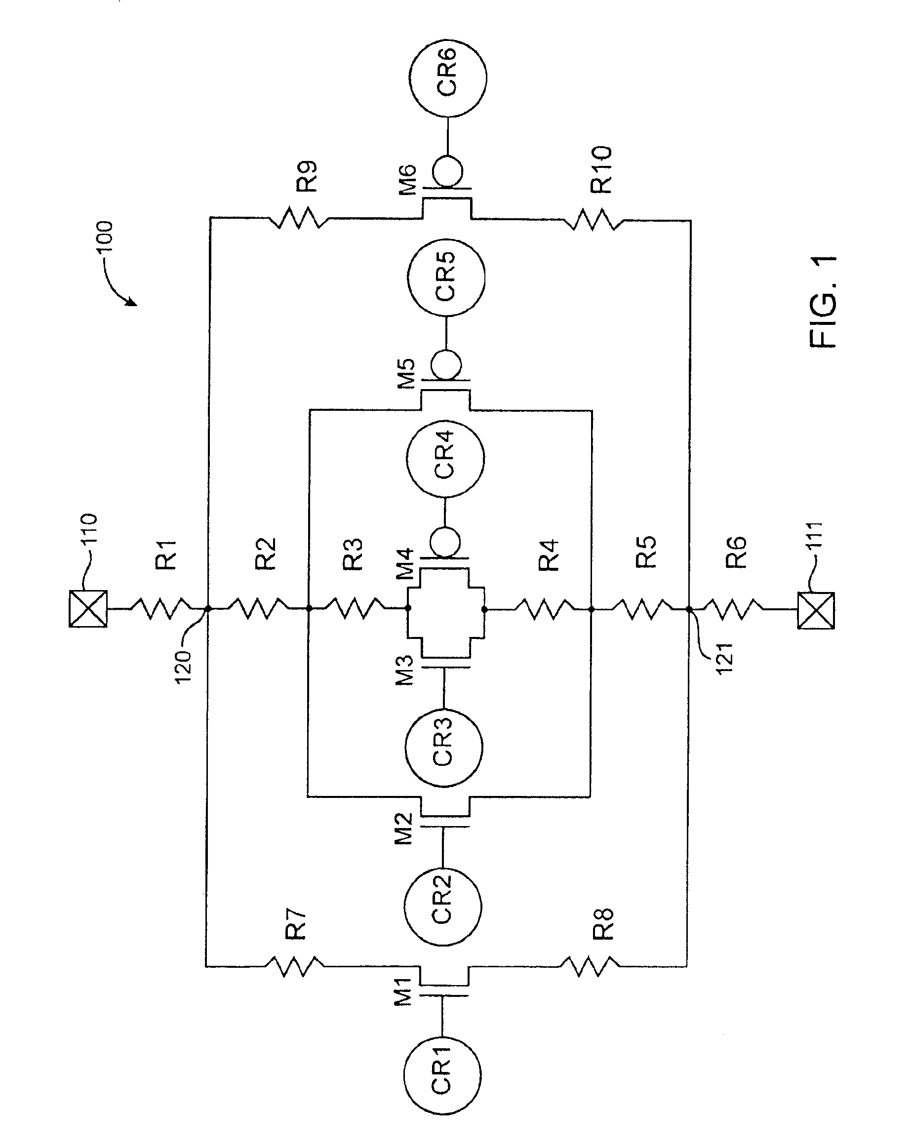
[0012]FIG. 1 illustrates the present invention. Impedance termination circuit 100 of FIG. 1 is an on-chip circuit that is coupled between two differential IO pins 110-111. Circuit 106 can be formed on an integrated circuit such as an ASIC, a programmable logic device, a field programmable gate array, a programmable logic array, a configurable logic array, etc.

[0013]Impedance termination circuit 100 includes resistors R1-R10 and field-effect transistors M1-M6. Any suitable resistor values and transistor sizes can be used in an impedance termination circuit of the present invention. The gates of transistors M1-M6 are coupled to six different memory cells CR1-CR6, respectively. Each of transistors M1-M6 is turned ON and OFF separately by bits stored in memory cells CR1-CR6.

[0014]Transistors M1-M6 can be turned ON and OFF by setting the values of the bits stored in memory cells CR1-CR6. Memory cells CR1-CR6 can be programmed by a user of the integrated circuit or by a manufacturer of th...

second embodiment

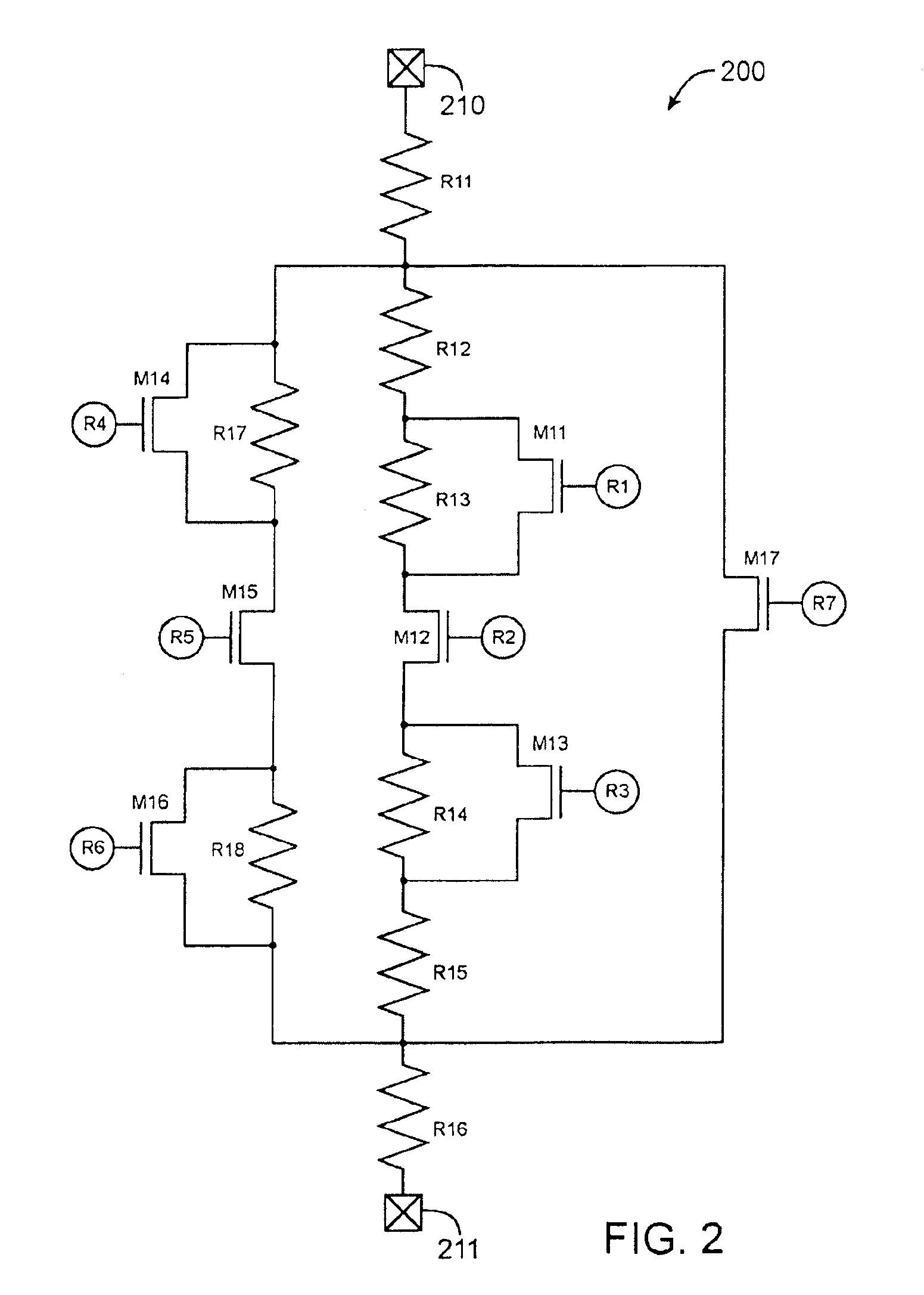
[0027]FIG. 2 illustrates the present invention. Impedance termination circuit 200 of FIG. 2 includes resistors R11-R18 and n-channel transistors M11-17. N-channel transistors M11-M17 are controlled by memory cells R1-R7, respectively. A user or a manufacturer stores bits (voltages) in memory cells R1-R7 to select the impedance termination of circuit 200.

[0028]If desired, any of n-channel transistors M11-M17 can be substituted for p-channel transistors. Circuit 200 is coupled between differential IO pins 210-211. Transistors M12, M15, and M17 can be turned OFF to create an infinite impedance (an open circuit condition) in circuit 200.

[0029]When transistors M11, M13, M15, and M17 are OFF, the total resistance of circuit 200 is R11+R12+R13+R14+R15+R16+RM12. Any appropriate resistance values can be selected for R11-R18. Any one or more of transistors M11-M17 can be turned ON to reduce the resistance of circuit 200. For example, transistor M11 can be turned ON to reduce the net resistanc...


PUM


Abstract

The circuits and methods are provided for impedance termination on an integrated circuit. A network of resistors are formed on an integrated circuit (IC) to provide on-chip impedance termination to differential input / output (IO) pins. Transistors are coupled in the network of termination resistors. The transistors provide additional termination impedance to the differential IO pins. The transistors can be turned ON or OFF separately to change the impedance termination.

Description

BACKGROUND OF THE INVENTION[0001]The present invention relates to techniques for providing on-chip termination impedance, and more particularly, to techniques for providing on-chip termination impedance to differential input / output pins.[0002]Integrated circuits have input / output (IO) pins that are used to transmit signals into and out of the circuit. An external termination resistor is usually coupled to each IO pin to provide impedance termination. An impedance termination resistor reduces reflection of input signals on signal lines coupled to the IO pin.[0003]However, external resistors typically use a substantial amount of board space. Therefore, it would be desirable to provide a technique for providing impedance termination for IO pins in an integrated circuit that does not occupy as much board space.[0004]Prior art integrated circuit have provided on-chip termination impedance by coupling a field-effect transistor to an IO pin. The gate voltage of the transistor is controlled...

Claims


Application Information

Patent Timeline
IPC IPC(8): H03K19/003H04L25/02
CPCH04L25/0278
Inventor WANG, BONNIE I.SUNG, CHIAKANGNGUYEN, KHAI
Owner ALTERA CORP
Learn More