Polynorbornene foam insulation for integrated circuits

a polynorbornene foam and integrated circuit technology, applied in the direction of electrical equipment, semiconductor devices, semiconductor/solid-state device details, etc., can solve the problems of limiting the minimum feature size that is operatively achievable, and affecting the efficiency of the conductive layer

Inactive Publication Date: 2005-05-10
MICRON TECH INC
View PDF99 Cites 21 Cited by
  • Summary
  • Abstract
  • Description
  • Claims
  • Application Information

AI Technical Summary

Benefits of technology

[0008]The invention includes methods of providing foamed polynorbornene insulating material for use with an integrated circuit device, as well as apparatus and systems making use of such foamed polynorbornene insulating materials. The methods include forming a layer of polynorbornene material and converting at least a portion of the layer of polynorbornene material to a foamed polynorbornene material, such as by exposing the layer of polynorbornene material to a supercritical fluid. The foamed polynorbornene material can provide electrical insulation between conductive layers of the integrated circuit device.

Problems solved by technology

As the minimum feature size in semiconductor integrated circuits decreases, however, capacitive coupling between adjacent conductive layers is becoming problematic.
In particular, for example, capacitive coupling between metal lines in the metallization level of integrated circuits limits the minimum feature size that is operatively achievable.
Nevertheless, the use of air as an insulating material, such as provided using an air bridge, has drawbacks.
For example, integrated circuit structures utilizing air insulation lack mechanical strength and protection from their environment.
However, porous silica xerogel film has a tendency to absorb water during processing.
The water absorbed during processing is released during aging, resulting in cracking and a pulling away of the porous silica xerogel film from the substrate on which it is applied.
Even when nonporous SiO2 is utilized, as the minimum feature size within an integrated circuit decreases, significant stress develops at the interface between the SiO2 and metal on which SiO2 is commonly formed, causing potentially detrimental disruptions in the electrical performance of the integrated circuit.
In contrast, the relatively low tensile yield strength of the metallization layer promotes its rupture, leading to integrated circuit failure.
The use of such foamed polymers, however, has been limited to electronic packaging applications and multichip module applications for microwave substrates.
Multichip module processing is not suitable for use in semiconductor fabrication because in multichip module processing, a metal insulator “sandwich” is formed as a unit and is then applied to a surface.

Method used


Image

  • Polynorbornene foam insulation for integrated circuits
  • Polynorbornene foam insulation for integrated circuits
  • Polynorbornene foam insulation for integrated circuits

Examples


Embodiment Construction

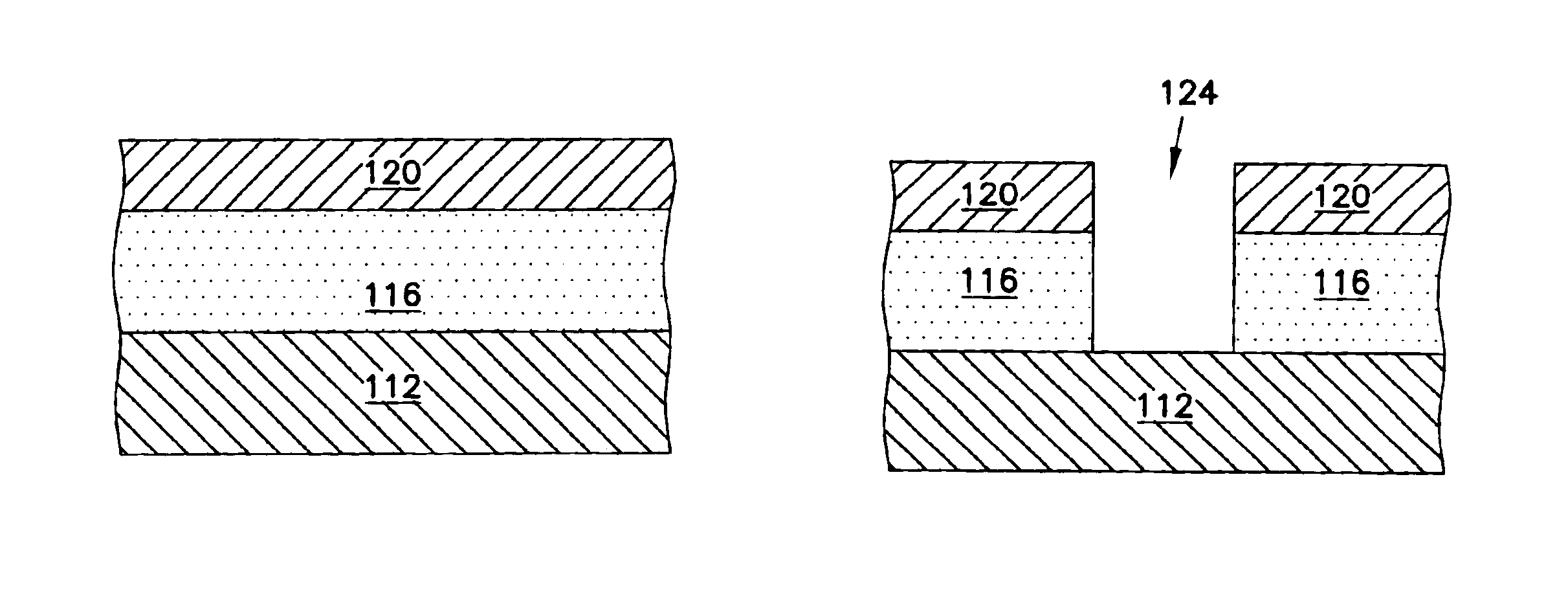
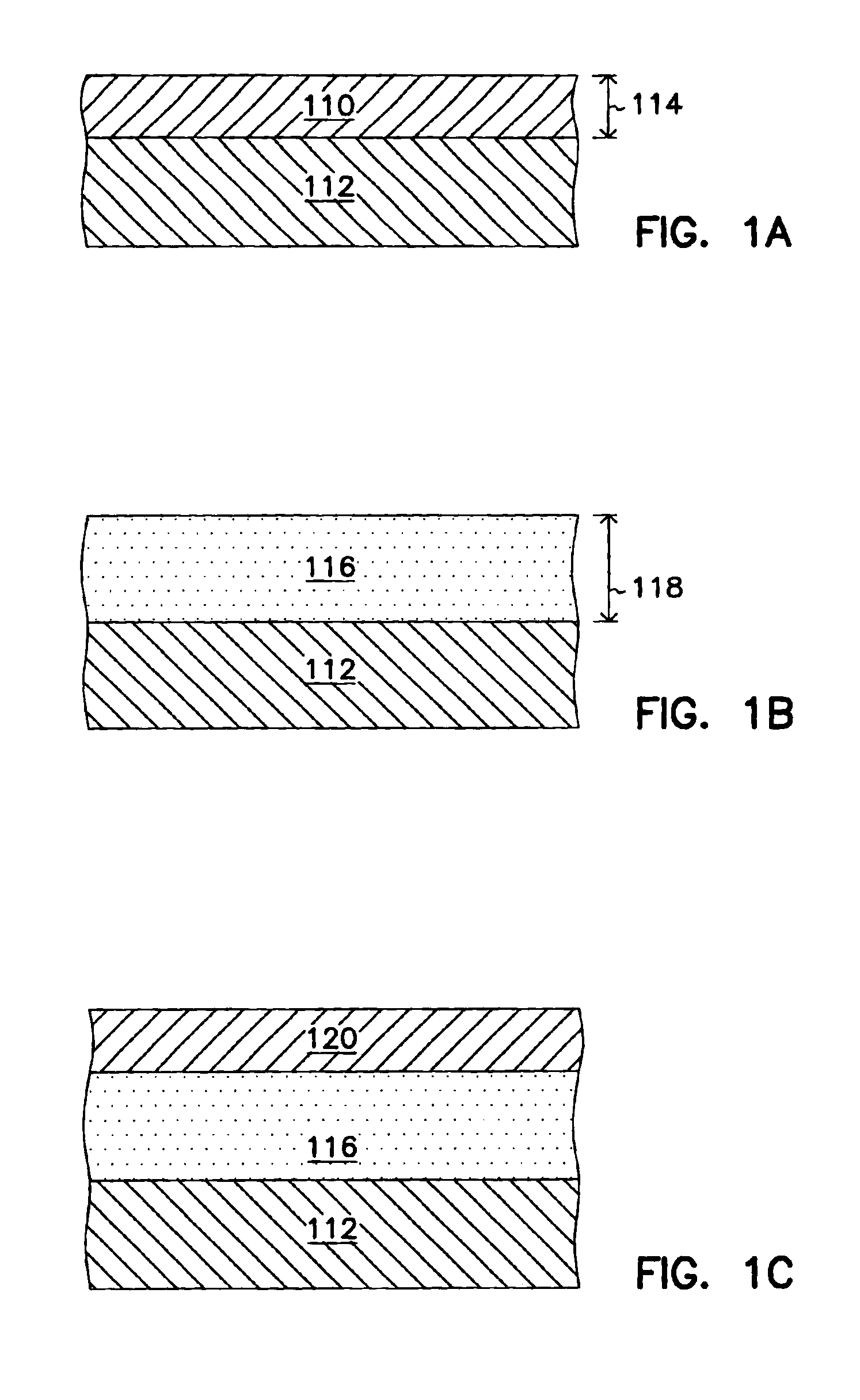
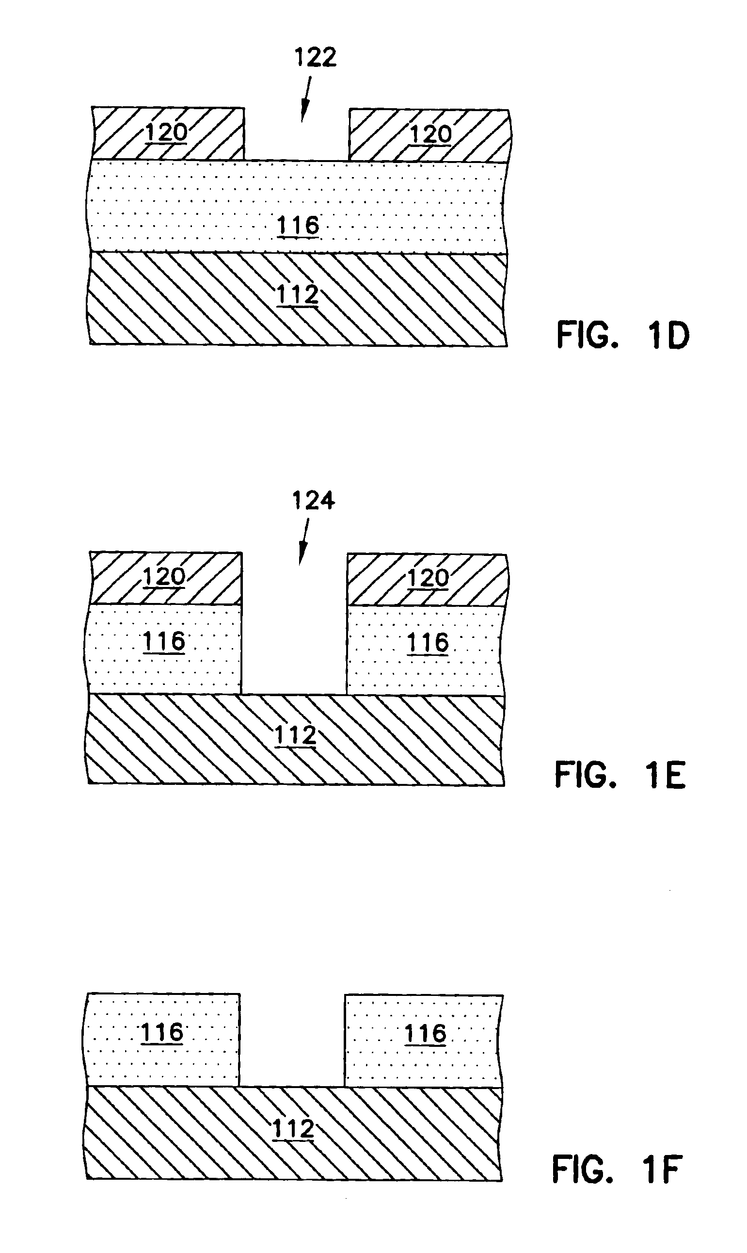
[0032]In the following detailed description of the preferred embodiments, reference is made to the accompanying drawings which form a part hereof, and in which is shown by way of illustration specific embodiments in which the inventions may be practiced. These embodiments are described in sufficient detail to enable those skilled in the art to practice the invention, and it is to be understood that other embodiments may be utilized and that process, electrical or mechanical changes may be made without departing from the scope of the present invention. The terms wafer and substrate used in the following description include any base semiconductor structure. Both are to be understood as including silicon-on-sapphire (SOS) technology, silicon-on-insulator (SOI) technology, thin film transistor (TFT) technology, doped and undoped semiconductors, epitaxial layers of a silicon supported by a base semiconductor structure, as well as other semiconductor structures well known to one skilled i...


PUM


Abstract

Methods of providing foamed polynorbornene insulating material for use with an integrated circuit device, as well as apparatus and systems making use of such foamed polynorbornene insulating materials. The methods include forming a layer of polynorbornene material and converting at least a portion of the layer of polynorbornene material to a foamed polynorbornene material, such as by exposing the layer of polynorbornene material to a supercritical fluid. The foamed polynorbornene material can provide electrical insulation between conductive layers of the integrated circuit device.

Description

TECHNICAL FIELD[0001]The present invention relates generally to development and fabrication of integrated circuits, and in particular to insulation techniques using polynorbornene foam as an insulating material in the development and fabrication of integrated circuits, as well as apparatus making use of such integrated circuits.BACKGROUND[0002]To meet demands for faster processors and higher capacity memories, integrated circuit (IC) designers are focusing on decreasing the minimum feature size within integrated circuits. By minimizing the feature size within an integrated circuit, device density on an individual chip increases exponentially, as desired, enabling designers to meet the demands imposed on them. As the minimum feature size in semiconductor integrated circuits decreases, however, capacitive coupling between adjacent conductive layers is becoming problematic. In particular, for example, capacitive coupling between metal lines in the metallization level of integrated circ...

Claims


Application Information

Patent Timeline
Patent Type & Authority Patents(United States)
IPC IPC(8): H01L21/02H01L23/52H01L23/28H01L23/31H01L23/532H01L21/312H01L21/70H01L21/8244H01L21/316H01L21/8242
CPCC08L65/00H01L21/312H01L21/7682H01L23/3171H01L23/5329H01L27/105H01L27/1052H01L2924/0002H01L21/31695H01L23/5222H01L27/10873H01L27/11H01L2924/19041H01L2924/00H01L2221/1047H01L21/02282H01L21/02118H01L21/02203H10B99/00H10B12/05H10B10/00H01L21/02345H01L21/02348
Inventor FARRAR, PAUL A.
Owner MICRON TECH INC
Why Eureka
Try Eureka