Memory module

a memory module and module technology, applied in the field of memory modules, can solve the problem of limiting the ability to reduce the size of the memory module to accommodate smaller system implementations, and achieve the effect of reducing the height of the longitudinal edge of the pcb

Inactive Publication Date: 2005-05-10
SAMSUNG ELECTRONICS CO LTD
View PDF19 Cites 53 Cited by
  • Summary
  • Abstract
  • Description
  • Claims
  • Application Information

AI Technical Summary

Benefits of technology

[0016]In the connector, multiple connection pads are electrically connected to the memory chip pads. The connection pads are arranged at regular intervals along the longitudinal edge of the connector and are constructed of thin metal panels designed to help exchange electrical si

Problems solved by technology

This memory module configuration increases the memory capacity of the system but limits the a

Method used


Image

  • Memory module
  • Memory module
  • Memory module

Examples


Embodiment Construction

[0023]Various embodiments of the present invention now will be described more fully with reference to the accompanying drawings. It should be noted, however, that the principles and aspects of the present invention set forth herein may be embodied in many different forms and should not be construed as being limited to the specific embodiments disclosed. These embodiments are provided by way of example and not of limitation.

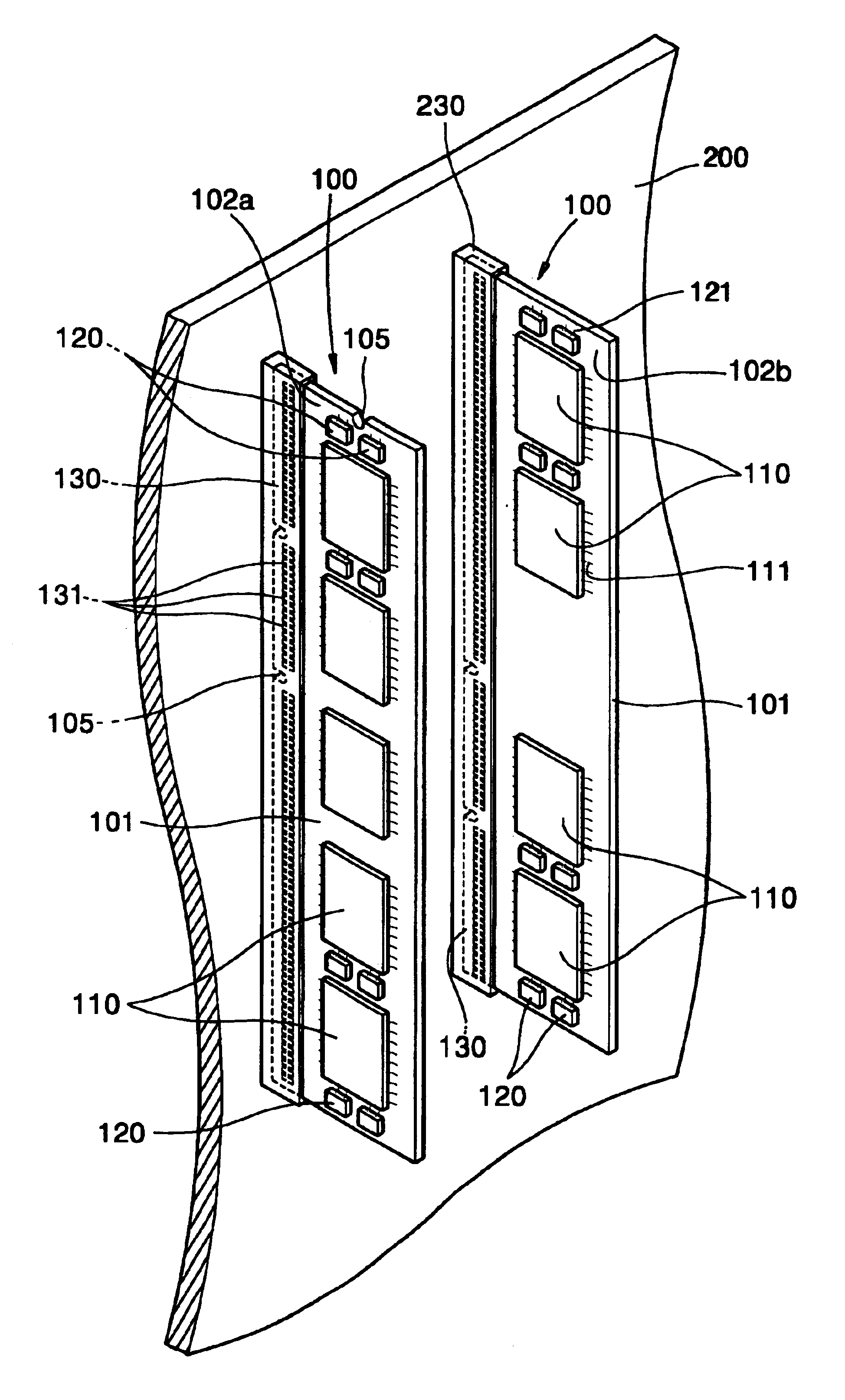
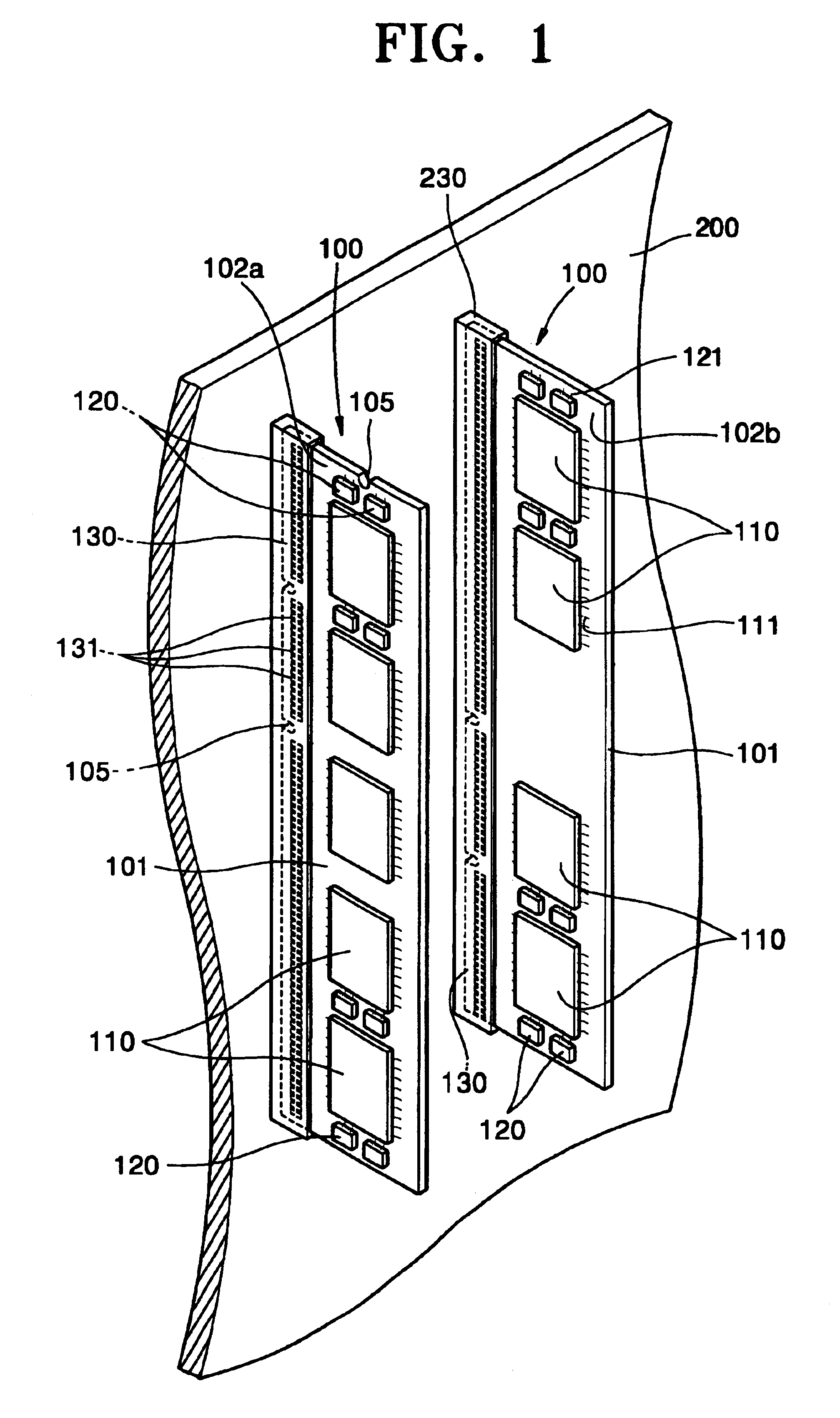
[0024]FIG. 1 is an elevated perspective view of a computing device 200 equipped with memory modules 100 constructed according to a preferred embodiment of the present invention. To illustrate both sides of the memory module 100, a front side 102a of the memory module 100 is shown on the left, and a rear side 102b of the memory module 100 is shown on the right.

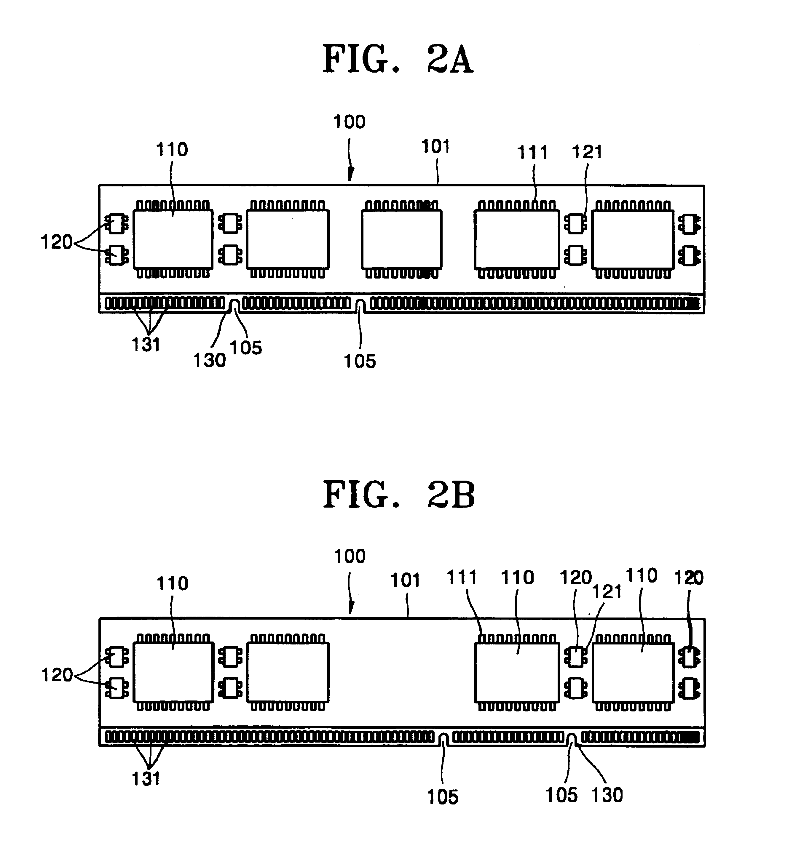
[0025]Referring to FIG. 1, the memory module 100 constructed according to a preferred embodiment of the present invention includes a rectangular, panel-type printed circuit board (PCB) 101. Multiple memory ch...


PUM


Abstract

A memory module preferably includes a printed circuit board (PCB) panel having multiple memory chip pad groups arranged on both sides thereof. Each memory chip pad group preferably includes multiple pads that correspond to lead lines of multiple memory chips arranged on the PCB panel. Connectors are preferably formed along an edge of the PCB panel to electrically connect the memory chip pad groups to an external device. Multiple damping chip pad groups preferably include built-in damping chips. One or more of the damping chip pad groups are preferably arranged adjacent to a lateral edge of one or more of the memory chips. The damping chip pad groups can electrically connect the connectors to the memory chip pad groups and dampen the signal noises.

Description

CROSS REFERENCE[0001]This application claims priority from Korean Patent Application No. 2001-55463, filed Sep. 10, 2001, the contents of which are hereby incorporated by reference in their entirety.BACKGROUND OF THE INVENTION[0002]1. Field of the Invention[0003]The present invention relates to a memory module including a printed circuit board (PCB), and more particularly, to a volatile memory module and PCB such as a Dynamic Random Access Memory (DRAM) or a Static Random Access Memory (SRAM) module.[0004]2. Description of Related Art[0005]A conventional memory module configured for installation in a personal computer (PC), a system server, or a communication switching system typically includes an off-chip printed circuit board (PCB) equipped with a memory integrated circuit (IC). The memory module further typically includes a connector for connecting the memory module to an external device. The connector exchanges an electrical data query (DQ) signal with the external device to rea...

Claims


Application Information

Patent Timeline
IPC IPC(8): G11C5/02G11C5/04H05K1/02H01L25/00H05K7/10
CPCG11C5/04H05K1/023H05K1/0231H05K1/0246H05K2201/10022H01L2924/0002H05K2201/10522H05K2201/10689H01L2924/00H05K7/10
Inventor KO, KI-HYUNKIM, KWANG-SEOP
Owner SAMSUNG ELECTRONICS CO LTD
Why Eureka
Try Eureka