Substrate bonding apparatus for liquid crystal display device panel

a technology of liquid crystal display and substrate, which is applied in the field of substrate bonding apparatus for liquid crystal display device panel, can solve the problems of difficult implementation of large-sized display screen, low image quality of lcd device, and low definition and high luminance, so as to reduce fabrication time and power consumption

a technology of liquid crystal display and substrate, which is applied in the field of substrate bonding apparatus for liquid crystal display device panel, can solve the problems of difficult implementation of large-sized display screen, low image quality of lcd device, and low definition and high luminance, so as to reduce fabrication time and power consumption

US6892769B2Active Publication Date: 2005-05-17LG DISPLAY CO LTD

Image

  • Substrate bonding apparatus for liquid crystal display device panel
  • Substrate bonding apparatus for liquid crystal display device panel
  • Substrate bonding apparatus for liquid crystal display device panel

Examples


Embodiment Construction

[0026]Reference will now be made in detail to the preferred embodiments of the present invention, examples of which are illustrated in the accompanying drawings.

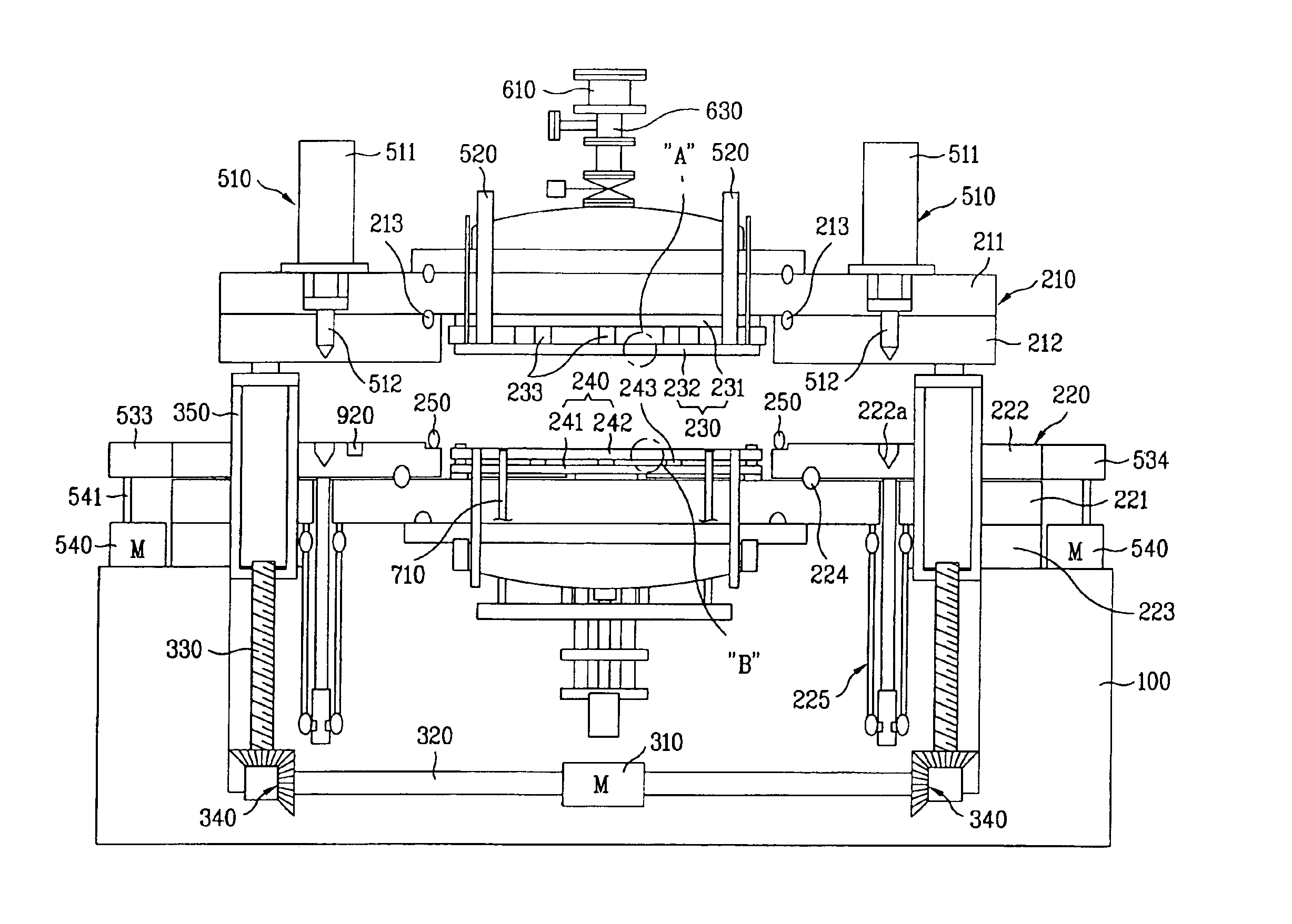
[0027]FIG. 3 is a cross sectional view of an exemplary substrate bonding apparatus for fabricating an LCD panel according to the present invention. In FIG. 3, a substrate bonding apparatus may include a base frame 100, an upper chamber unit 210, a lower chamber unit 220, an upper stage 230, and a lower stage 240. The substrate bonding apparatus may also include an interlocking system 510 and a support system 710. In addition, although not specifically shown, the substrate bonding apparatus may include a chamber moving system, a sealing system, alignment cameras, an alignment system, a vacuum pumping system, and high and low vacuum chambers.

[0028]The base frame 100 may be fixed to a floor structure (not shown), and may form an exterior of the substrate bonding apparatus. In addition, the base frame 100 may simultaneously supp...


PUM

PropertyMeasurementUnit
pressureaaaaaaaaaa
vacuumaaaaaaaaaa
heightaaaaaaaaaa

Abstract

A substrate bonding apparatus for a liquid crystal display device panel includes an upper chamber plate, a lower chamber plate opposing the upper chamber plate, an upper low vacuum chamber provided on the upper chamber plate, a lower low vacuum chamber provided on a rear surface of the lower chamber plate, a sealing member provided on the lower chamber plate, the sealing member projecting from a top surface of the lower chamber plate at a predetermined height to contact the upper chamber plate to form a high vacuum chamber therein, at least two holes provided in each of the upper and lower chamber plates, at least two flow shut-off systems shutting off each of the holes, vacuum pumping system for reducing pressures of the upper and lower low vacuum chambers to low vacuum states, and reducing the high vacuum chamber to a high vacuum state, and upper and lower stages provided to upper and lower chamber plates, respectively, within an inside space of the high vacuum chamber to affix first and second substrates of the liquid crystal display device panel, respectively.

Description

[0001]The present invention claims the benefit of Korean Patent Application Nos. P2003-43489, filed in Korea on Jun. 30, 2003, and P2004-35191, filed in Korea on May 18, 2004 which are hereby incorporated by reference.BACKGROUND OF THE INVENTION[0002]1. Field of the Invention[0003]The present invention relates to an apparatus for bonding substrates together, and more particularly, to a substrate bonding apparatus for a liquid crystal display (LCD) device panel.[0004]2. Discussion of the Related Art[0005]As demand for displaying various types of visual information increases, different types of display devices, such as LCD devices, plasma display panel (PDP) devices, electro-luminescent display (ELD) devices, and vacuum fluorescent display (VFD) devices, are being developed. Among these different types of display devices, the LCD devices are commonly used in portable display devices and are used to replace cathode ray tube (CRT) devices because of their excellent image quality, light ...

Claims


Application Information

Patent Timeline
17 May 2005
Publication
US6892769B2
IPC
B65B1/04; G02F1/13; G02F1/1333; G02F1/1339; B29C43/56; B29C65/00; B32B37/10; B67C3/00; G02F1/1341; H01L21/00; H01L21/683
CPC
B29C43/56; B32B37/10; B29C2043/3602; B29C2043/561; H01L21/6838; B32B2457/20; B32B2457/202; G02F1/1341
Inventors
HONG, SANG PYO