Conductive polishing pad with anode and cathode

a polishing pad and conductive technology, applied in the field of polishing pads, can solve the problems of inability to carry out ecmp, the mechanical aspect of the cmp is reaching the limit of its ability to planarize such ic substrates, and the delamination and fracture of the underlayer cap and dielectric material,

Inactive Publication Date: 2005-05-17
ROHM & HAAS ELECTRONICS MATERIALS CMP HLDG INC
View PDF16 Cites 78 Cited by
  • Summary
  • Abstract
  • Description
  • Claims
  • Application Information

AI Technical Summary

Benefits of technology

[0030]One aspect of the invention is a polishing pad that includes one or more anodes formed in the polishing pad at or near a polishing surface of the pad, a

Problems solved by technology

Moreover, the mechanical aspect of CMP is reaching the limit of its ability to planarize such IC substrates because the layers cannot handle the mechanical stress of polishing.
In particular, delamination and fracture of the underlayer cap and dielectric material occurs during CMP due to frictional stress induced by the physical contact between the polishing

Method used


Image

  • Conductive polishing pad with anode and cathode
  • Conductive polishing pad with anode and cathode
  • Conductive polishing pad with anode and cathode

Examples


Embodiment Construction

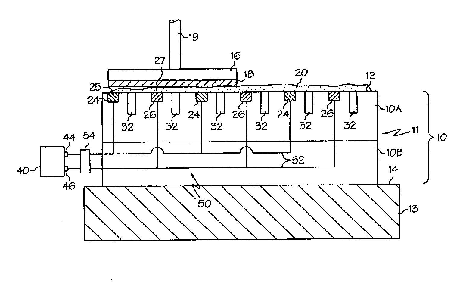
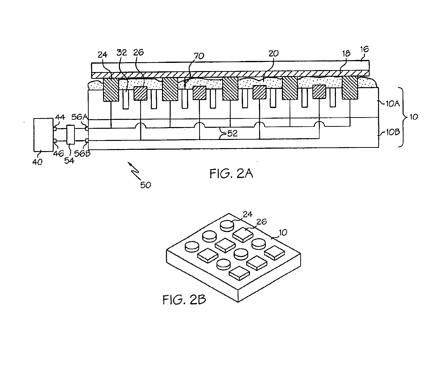
[0032]In the description below, a generalized embodiment of the conductive polishing pad of the present invention is first described. Then several specific embodiments of different polishing pad geometries are set forth for the sake of illustration. An electrical connector system for maintaining electrical connections between the anodes, cathodes and current supply when the polishing pad is in motion relative to the current supply is then described. Next, an embodiment of a polishing / planarizing system that utilizes the conductive polishing pad of the present invention is then described.

[0033]The polishing pad and systems described hereinbelow are suitable for polishing or planarizing various types of semiconductor substrates and wafers that have an uppermost metal layer, or metal portions on the surface to be polished. The present invention is also well-suited for polishing relatively brittle substrates (e.g., gallium arsenide, silicon-on-insulator, low k dielectrics, etc.) because...


PUM

PropertyMeasurementUnit
Lengthaaaaaaaaaa
Lengthaaaaaaaaaa
Lengthaaaaaaaaaa

Abstract

A conductive polishing pad that includes one or more anodes and one or more cathodes formed at or near the polishing surface of a polishing pad. The anodes and cathodes are connected to a wiring network that is part of an electrical connector system that allows for a current source to be connected to the polishing pad and provide a current to the anodes and cathodes even if the polishing pad is moving relative to the current source. An electrolytic polishing fluid introduced between the polishing surface and the metal layer of a wafer forms an electrical circuit between the anode, cathode and the metal layer. The conductive polishing pad allows for electrochemical mechanical polishing (ECMP) to be performed on a conventional chemical mechanical polishing (CMP) tool.

Description

BACKGROUND OF THE INVENTION[0001]The invention relates to polishing pads for chemical mechanical planarization (CMP) and electrochemical mechanical planarization (ECMP), and in particular relates to conductive polishing pads for same.[0002]In the fabrication of integrated circuits and other electronic devices, multiple layers of conducting, semiconducting, and dielectric materials are deposited on or removed from the surface of a semiconductor wafer. Thin layers of conducting, semiconducting, and dielectric materials are deposited by a number of deposition techniques. Common deposition techniques include physical vapor deposition (PVD), also known as sputtering, chemical vapor deposition (CVD), plasma-enhanced chemical vapor deposition (PECVD), and electrochemical plating (ECP).[0003]As layers of materials are sequentially deposited and removed, the uppermost surface of the wafer becomes non-planar. Because subsequent semiconductor processing (e.g., metallization) requires the wafer...

Claims


Application Information

Patent Timeline
IPC IPC(8): B24B37/04B23H5/08C25F7/00
CPCB23H5/08B24B37/046B24B37/24C25F7/00B24B37/20Y10S451/908
Inventor SO, JOSEPH K.
Owner ROHM & HAAS ELECTRONICS MATERIALS CMP HLDG INC
Why Eureka
Try Eureka