Semiconductor integrated circuit device, process for fabricating the same, and apparatus for fabricating the same

a technology of integrated circuit devices and semiconductors, applied in the field of semiconductor technology, can solve the problems of insufficient retention of memory cell area and memory cell separating area, inability to highly integrate dram, and inability to retain cell area, etc., to achieve the effect of reducing displacement of alignment, and improving the degree of integration of semiconductor integrated circuit devices

Inactive Publication Date: 2005-05-17
RISING SILICON
View PDF59 Cites 5 Cited by
  • Summary
  • Abstract
  • Description
  • Claims
  • Application Information

AI Technical Summary

Benefits of technology

[0008]In the DRAM, the separations of the memory cells are accomplished at present at an element separating insulating film and channel stopper regions. The element separating insulating film is formed by oxidizing the principal surface of the inactive regions of the semiconductor substrate by using a non-oxidizable mask (of a silicon nitride film) formed over the principal surface of the active regions of the semiconductor substrate. On the other hand, the channel stopper regions are formed of an impurity such as B, which is introduced into the principal surface portions of the active regions (i.e., only the memory cell array) and the inactive regions of the semiconductor substrate. This impurity is introduced, after the element separating insulating film has been formed, by the ion implantation method using such a high energy as to transmit the element separating insulating film. More specifically, the impurity introduced into the principal surface portions of the inactive regions of the semiconductor substrate below the element separating insulating film is formed as the aforementioned channel stopper regions. Since the impurity thus introduced into the principal surface portions of the active regions of the semiconductor substrate is introduced into deeper regions than the impurity introduced into the principal surface portions of the inactive regions, it will not adversely affect the memory cells. The process of forming the channel stopper regions using the ion implantation method using that high energy is featured in that it can reduce the narrow channel effect of the memory cell selecting MISFET. Specifically, the aforementioned forming process can form the channel stopper regions in self-alignment with the element separating insulating film so that it can reduce the amount of diffusion of the impurity for forming the channel stopper regions to the active regions.
[0046]According to the aforementioned means (33), the intermediate conducting film of the peripheral circuit can be formed at the step of forming the intermediate conducting film formed in the memory cells of the DRAM to reduce the number of fabrication steps.

Problems solved by technology

However, the DRAM being developed by us is intended to have a capacity as large as 16 [Mbits] so that it cannot retain the memory cell area and the memory cell separating area sufficiently.
As a result, the memory cell area can neither be retained, not can be shrunk the separating area of the memory cells, thus raising a problem that the DRAM cannot be highly integrated.

Method used


Image

  • Semiconductor integrated circuit device, process for fabricating the same, and apparatus for fabricating the same
  • Semiconductor integrated circuit device, process for fabricating the same, and apparatus for fabricating the same
  • Semiconductor integrated circuit device, process for fabricating the same, and apparatus for fabricating the same

Examples


embodiment i

(Embodiment I)

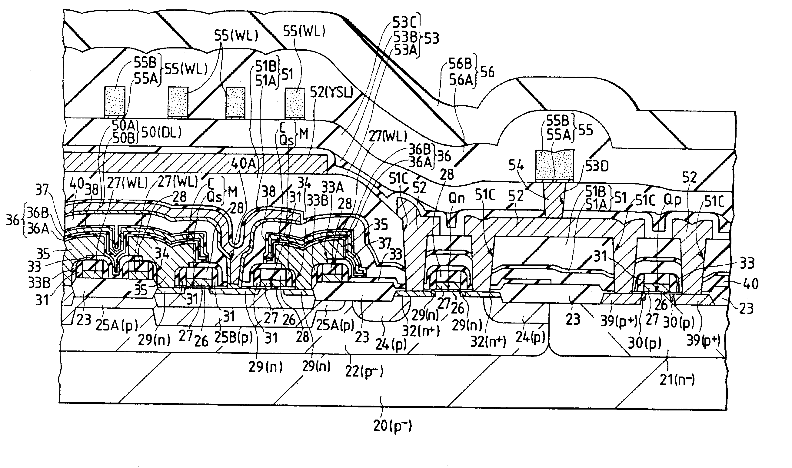
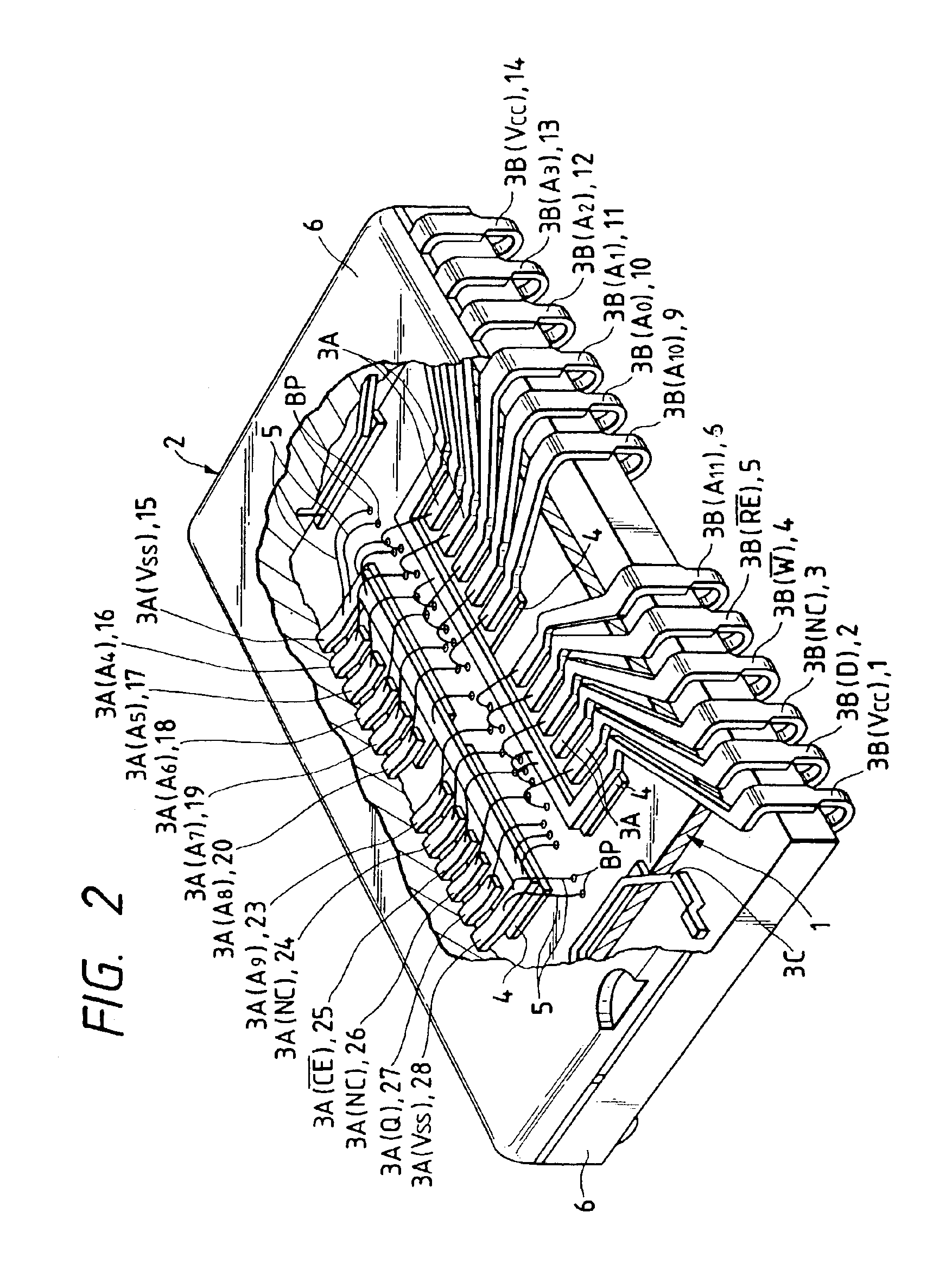
[0098]A resin-sealed type semiconductor device for sealing a DRAM according to the embodiment I of the present invention will be described with reference to FIG. 2 (of partially sectional, perspective view).

[0099]As shown in FIG. 2, the DRAM (of a semiconductor pellet) 1 is sealed by an SOJ (Small Out-line J-bend) type resin-sealed type semiconductor device 2. The DRAM 1 is made to have a large capacity of 16 [Mbits]×1 [bit] and a rectangular top plan size of 16.48 [mm]×8.54 [mm]. This DRAM 1 is sealed by the resin-sealed type semiconductor device 2 of 400 [mil].

[0100]The aforementioned DRAM 1 has its principal surface arranged mainly with memory cell arrays and peripheral circuits. Each of the memory cell arrays is arranged, as will be described in detail, with a matrix shape of a plurality memory cells (or storage elements) for storing an information of 1 [bit]. The aforementioned peripheral circuits are composed of direct peripheral circuits and indirect peripheral ...

embodiment ii

(Embodiment II)

[0305]The present embodiment II is a second embodiment of the present invention, which adopts the leaf type in the step of burying the transition-metal film in the connecting holes for connecting the different wiring layers, so as to improve the production yield of the DRAM 1 of the foregoing embodiment I.

[0306]An essential portion of the DRAM 1 according to the embodiment II of the present invention is shown in FIG. 56 (presenting the essential portion in section).

[0307]In the DRAM 1, as shown in FIG. 56, a transition-metal film 83 buried in a connecting hole 82A formed in an interlayer insulating film 82 is connected with a wiring line 81 formed over an under insulating film 80. The wiring line 81 is formed of an aluminum film or its alloy film. The interlayer insulating film 82 is formed of either a single layer of a silicon oxide film or a composite composed mainly of the former. The transition-metal film 83 buried in the connecting hole 82A is formed of the W fil...

embodiment iii

(Embodiment III)

[0318]The present embodiment III is directed to a third embodiment of the present invention, in which the transition-metal film is buried in the connecting hole for connecting the semiconductor substrate and the wiring layer, although having different a structure from that of the DRAM 1 of the foregoing embodiment II, and in which the leaf type is adopted in the burying step.

[0319]An essential portion of the DRAM 1 according to the embodiment III of the present invention is shown in FIG. 59 (presenting the essential portion in section).

[0320]In the DRAM 1 of the present embodiment III, as shown in FIG. 59, with the n+-type semiconductor region 32 formed over in the principal portion of the p−-type well region 22, there is connected a transition-metal film 84 which is buried in the connecting hole 80A formed in the interlayer insulating film 80. The n+-type semiconductor region 32 is made of silicon (Si), as has been described in connection with the foregoing embodime...


PUM

PropertyMeasurementUnit
aspect ratioaaaaaaaaaa
sizeaaaaaaaaaa
operating voltageaaaaaaaaaa

Abstract

Herein disclosed is a semiconductor integrated circuit device fabricating process for forming MISFETs over the principal surface in those active regions of a substrate, which are surrounded by inactive regions formed of an element separating insulating film and channel stopper regions, comprising: the step of for forming a first mask by a non-oxidizable mask and an etching mask sequentially over the principal surface of the active regions of the substrate; the step of forming a second mask on and in self-alignment with the side walls of the first mask by a non-oxidizable mask thinner than the non-oxidizable mask of the first mask and an etching mask respectively; the step of etching the principal surface of the inactive regions of the substrate by using the first mask and the second mask; the step of forming the element separating insulating film over the principal surface of the inactive regions of the substrate by an oxidization using the first mask and the second mask; and the step of forming the channel stopper regions over the principal surface portions below the element separating insulating film of the substrate by introducing an impurity into all the surface portions including the active regions and the inactive regions of the substrate after the first mask and the second mask have been removed.

Description

[0001]This application is a Continuation application of Ser. No. 09 / 899,921, filed Jul. 9, 2001, now U.S. Pat. No. 6,548,847; which is a Divisional application of Ser. No. 09 / 459,921, filed Dec. 14, 1999, now U.S. Pat. No. 6,342,412; which is a Continuation application of Ser. No. 08 / 943,729, filed Oct. 3, 1997, now U.S. Pat. No. 6,127,255; which is a Continuation application of Ser. No. 08 / 460,931, filed Jun. 5, 1995, now U.S. Pat. No. 5,811,316; and this application is a Continuation application of Ser. No. 08 / 458,481, filed Jun. 2, 1995, now Abandoned; and Ser. No. 08 / 460,931 and Ser. No. 08 / 458,481 are Divisional applications of Ser. No. 08 / 230,021, filed Apr. 19, 1994, now U.S. Pat. No. 5,557,147; which is a Divisional application of Ser. No. 07 / 954,142, filed Sep. 30, 1992, now U.S. Pat. No. 5,331,191; which is a Divisional application of Ser. No. 07 / 496,330, filed Mar. 20, 1990, now U.S. Pat. No. 5,202,275.BACKGROUND OF THE INVENTION[0002]The present invention relates to a se...

Claims


Application Information

Patent Timeline
Patent Type & Authority Patents(United States)
IPC IPC(8): G03F9/00G03F7/20H01L21/285H01L23/525H01L21/02H01L23/495H01L21/76H01L23/52H01L23/28H01L21/70H01L23/544H01L23/29H01L21/8242H01L23/532H01L21/768H01L21/8238H01L23/48H01L27/085H01L27/092H01L27/108H01L21/336H01L27/10H01L29/78
CPCG03F7/70333H01L21/28512H01L21/76H01L21/76801H01L21/76804H01L21/76831H01L21/76834H01L21/76838H01L21/76843H01L21/76877H01L21/823807H01L23/291H01L23/4951H01L23/5258H01L23/532H01L23/544H01L27/0922H01L27/10852H01L28/40G03F9/70H01L2924/01015H01L27/0928H01L27/10808H01L2223/54473H01L2224/48091H01L2224/48247H01L2224/4826H01L2924/01014H01L2924/01029H01L2924/01039H01L2924/01079H01L2924/04941H01L2924/12044H01L2924/14H01L2924/19041H01L2924/3025H01L2224/4569H01L2224/45565H01L24/45Y10S257/90H01L2224/45147H01L2224/45124H01L2224/45144H01L2924/01021H01L24/48H01L2924/00014H01L2924/12042H01L2924/12036H01L2924/181H01L2224/05554H01L2224/73215H10B12/31H10B12/033H01L2924/00H01L2224/05599H01L2924/00012H01L27/10
Inventor SUGIURA, JUNTSUCHIYA, OSAMUOGASAWARA, MAKOTOOOTSUKA, FUMIOTORII, KAZUYOSHIASANO, ISAMUOWADA, NOBUOHORIUCHI, MITSUAKITAMARU, TSUYOSHIAOKI, HIDEOOTSUKA, NOBUHIROSHIRAI, SEIICHIROUSAGAWA, MASAKAZUIKEDA, YOSHIHIROTSUNEOKA, MASATOSHIKAGA, TORUSHIMMYO, TOMOTSUGUOGISHI, HIDETSUGUKASAHARA, OSAMUENAMI, HIROMICHIWAKAHARA, ATSUSHIAKIMORI, HIROYUKISUZUKI, SINICHIFUNATSU, KEISUKEKAWASAKI, YOSHINAOTUBONE, TUNEHIKOKOGANO, TAKAYOSHITSUGANE, KEN
Owner RISING SILICON
Why Eureka
Try Eureka