Semiconductor device and preparation method thereof, and electronic apparatus

A technology of electronic devices and semiconductors, applied in semiconductor devices, semiconductor/solid-state device manufacturing, circuits, etc., can solve problems such as aggravated impacts

Active Publication Date: 2017-07-07
SEMICON MFG INT (SHANGHAI) CORP +1
View PDF6 Cites 0 Cited by
  • Summary
  • Abstract
  • Description
  • Claims
  • Application Information

AI Technical Summary

Problems solved by technology

[0004] Further, as the size of the period shrinks, the stress of the shallow trench isolation structure in the device will have a significant impact on the transistor

Method used


Image

  • Semiconductor device and preparation method thereof, and electronic apparatus
  • Semiconductor device and preparation method thereof, and electronic apparatus
  • Semiconductor device and preparation method thereof, and electronic apparatus

Examples


Embodiment 1

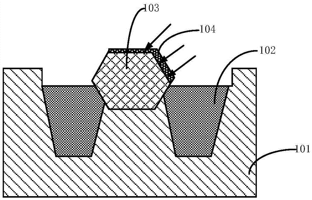
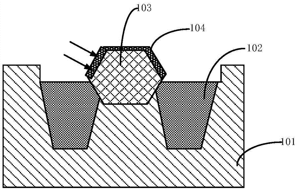
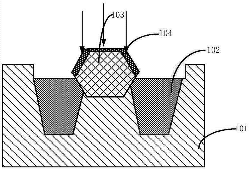
[0032] In order to solve the problems existing in the prior art in the present invention, a kind of preparation method of semiconductor device is provided, below in conjunction with attached Figures 1a-1d A specific embodiment of the present invention will be further described.

[0033] Step 101 is executed to provide a semiconductor substrate 101 on which a gate structure and Σ-shaped raised source and drain located on both sides of the gate structure are formed.

[0034] Specifically, refer to Figure 1a , a semiconductor substrate 101 is provided, and the semiconductor substrate 101 may be at least one of the materials mentioned below: silicon, silicon-on-insulator (SOI), silicon-on-insulator (SSOI), and the like.

[0035] In addition, an active region may be defined on the semiconductor substrate 101 . Other active devices may also be included on the active area, which are not marked in the shown figures for convenience.

[0036] Then a gate structure is formed on the s...

Embodiment 2

[0074] The present invention also provides a semiconductor device, which is prepared by the method described in the first embodiment. In the semiconductor device prepared by the method, an amorphous layer is formed on the inclined sidewall of the upper part of the Σ-shaped raised source and drain, which can reduce the Σ-shaped in the subsequent steps of LDD ion implantation and / or source-drain implantation. Raise the ion implantation depth at the edge of the source and drain, reduce the narrow channel effect, thereby lowering the threshold voltage and improving the performance and yield of semiconductor devices.

Embodiment 3

[0076] The present invention also provides an electronic device, including the semiconductor device described in the second embodiment. Wherein, the semiconductor device is the semiconductor device described in the second embodiment, or the semiconductor device obtained according to the preparation method described in the first embodiment.

[0077] The electronic device of this embodiment can be any electronic product or equipment such as mobile phone, tablet computer, notebook computer, netbook, game console, TV set, VCD, DVD, navigator, camera, video recorder, voice recorder, MP3, MP4, PSP, etc. , can also be any intermediate product including the semiconductor device. The electronic device according to the embodiment of the present invention has better performance due to the use of the above-mentioned semiconductor device.


PUM

PropertyMeasurementUnit
Thicknessaaaaaaaaaa

Abstract

The invention relates to a semiconductor device and a preparation method thereof, and an electronic apparatus. The method comprises the following steps: providing a semiconductor substrate, wherein a gate structure and a sigma-shaped elevated source and drain on the two sides of the gate structure are formed on the semiconductor substrate; and S2, performing amorphization ion implantation on the inclined sidewalls of the upper parts of the sigma-shaped elevated source and drain to form an amorphous layer on the inclined sidewalls in order to reduce the ion implantation depth of LDD ion implantation and/or source-drain implantation below the edges of the sigma-shaped elevated source and drain. According to the method, in the process of preparation, after the sigma-shaped elevated source and drain are formed, vertical or approximately vertical amorphization ion implantation is performed on the inclined sidewalls of the upper parts of the sigma-shaped elevated source and drain to form an amorphous layer on the inclined sidewalls in order to reduce the ion implantation depth at the edges of the sigma-shaped elevated source and drain in subsequent LDD ion implantation and/or source-drain implantation. Therefore, the performance and yield of the semiconductor device are improved.

Description

technical field [0001] The present invention relates to the field of semiconductors, in particular, the present invention relates to a semiconductor device, a preparation method thereof, and an electronic device. Background technique [0002] With the continuous development of semiconductor technology, the preparation of semiconductor devices tends to be miniaturized, and has been developed to the nanometer level, while the preparation process of conventional devices is gradually mature. As the size of semiconductor devices continues to shrink, the width of the gate continues to decrease. When the channel width of a field effect transistor is approximately equal to the width of the depletion layer of the source and drain junctions, it is a so-called "narrow channel" device. When the size of the device structure is reduced, not only the channel length becomes shorter, but also the width will be reduced in the same proportion, so narrow channel devices will appear. The phenom...

Claims


Application Information

Patent Timeline
IPC IPC(8): H01L21/265H01L29/04H01L29/08H01L21/336H01L29/78
CPCH01L29/04H01L29/0847H01L29/66568H01L29/7848H01L21/26506
Inventor 王冬江
Owner SEMICON MFG INT (SHANGHAI) CORP
Why Eureka
Try Eureka