Substrate with a flattening film, display substrate, and method of manufacturing the substrates

a technology of flattening film and substrate, which is applied in the direction of identification means, instruments, optics, etc., can solve the problems of unique disadvantage of tft, poor display quality, and leakage current of tft, and achieve the effect of reducing thickness and being easily mass-producibl

Inactive Publication Date: 2005-05-17
SHARP KK
View PDF6 Cites 14 Cited by
  • Summary
  • Abstract
  • Description
  • Claims
  • Application Information

AI Technical Summary

Benefits of technology

[0030]Conceived to address the foregoing conventional problems, the present invention has an object to suggest a substrate with a planarization film and a method of manufacturing such a substrate. In the substrate, the polished film and the polished portion are reduced in thickness and thereby only needs to meet less strict requirements as to uniformity in thickness of the polished film and that of the polished portion during the formation of a planarization film by CMP. The invention has another object to apply such a substrate and a method of manufacturing it in offering an easily mass-producible display and a method of manufacturing such a display.

Problems solved by technology

The TFT leaks current upon light exposure, which is a unique disadvantage to the TFT.
In liquid crystal displays, the photo-induced leak current results in poor contrast and increased crosstalk which in turn cause poor display quality.
The problems are particularly serious with liquid crystal displays in liquid crystal projectors in which the display is used under intense light.
The existence of irregularities is however a hindrance for a proper alignment treatment to be carried out where the irregularities cause abrupt changes in surface level.
The result is defective alignment of the liquid crystal.
Another problem arises if those parts where alignment is defective are shielded against light to ensure a good contrast level: the aperture ratio, and hence brightness, drops dramatically, especially in liquid crystal displays for the liquid crystal projector with small pixels.
A specific problem arises, in bringing the variations within a certain, restricted range: requirements are extremely high as to both the uniformity in thickness of the polished film 140 and the uniformity in thickness of the portion 141 polished and hence removed by CMP.
These requirements for excellent uniformity, i.e., such strict restrictions on the uniformity in the thickness of the polished film 140 and the uniformity in thickness of the portion 141 polished and hence removed by CMP that they fall within 1.5% as discussed here, presents a major obstacle in mass-producing liquid crystal displays.
Note that although these problems are unique to CMP and do not occur in SOG as a film planarization method, SOG has its own problems: the method is capable of smoothing out steps on the underlying surface only partially, not completely and not much reliable in a high intensity light environment, as when applied to projector panels, because of possible light-induced chemical reactions of an organic component leftover from the SOG process.

Method used


Image

  • Substrate with a flattening film, display substrate, and method of manufacturing the substrates
  • Substrate with a flattening film, display substrate, and method of manufacturing the substrates
  • Substrate with a flattening film, display substrate, and method of manufacturing the substrates

Examples


example 1

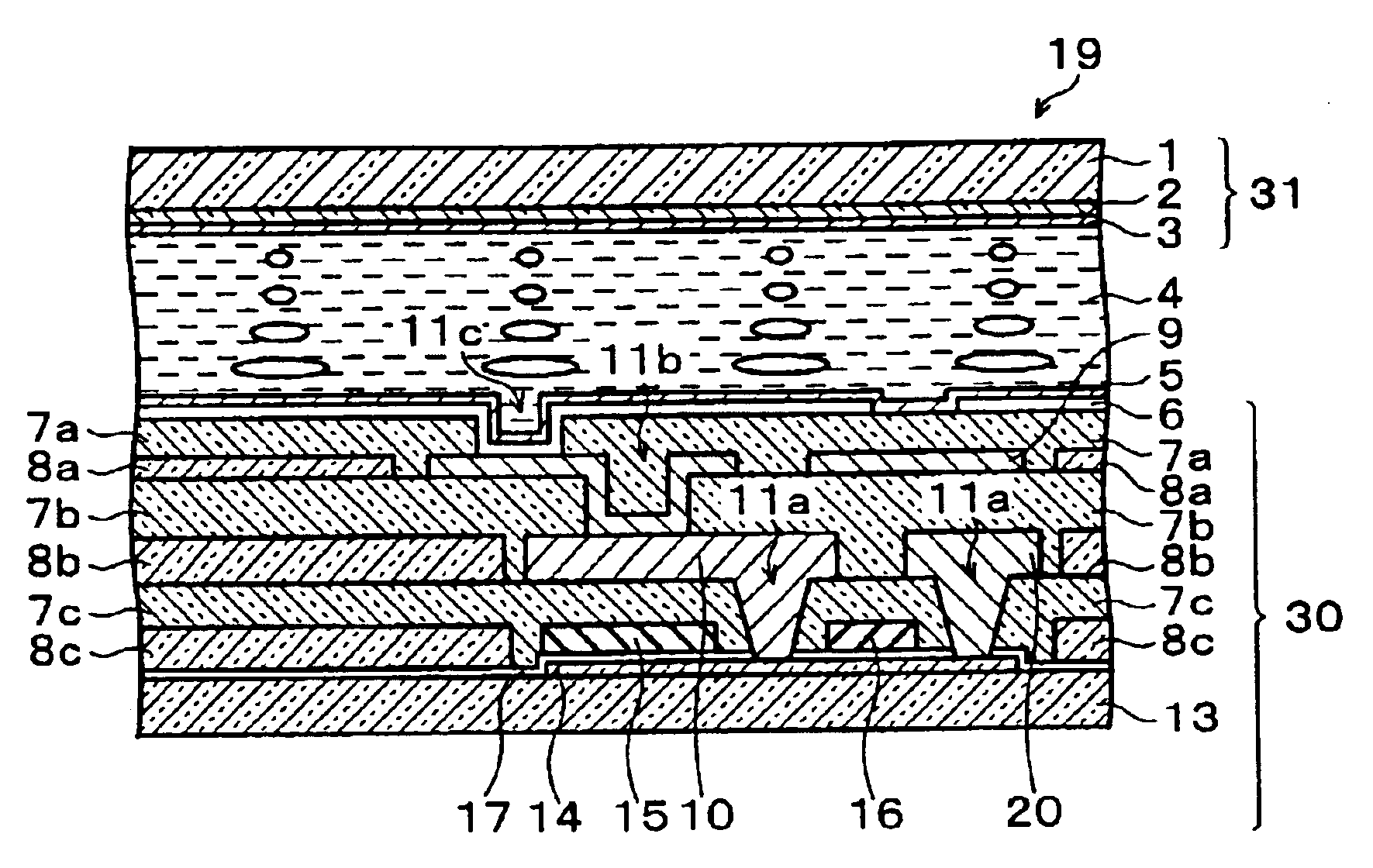
[0141]FIG. 1 shows an example case of a liquid crystal display including: thin film transistors, additional capacitances (electrodes), and transparent pixel electrodes provided at intersections of gate wires and signal wires crossing each other at right angles; a first light-shield film beneath the thin film transistors with an interlayer insulating film intervening there between; and a second light-shield film on top of the signal lines with an interlayer insulating film intervening there between, wherein each interlayer insulating film has an insulating film pattern and is planarized by CMP.

[0142]If any one of the interlayer insulating films has no insulating film pattern in relation to manufacturing cost and productivity, that interlayer insulating film may be subjected to a conventional method, such as simple CVD whereby an insulating film is deposited.

[0143](1) A film (50 nm) of polycrystalline Si doped with phosphorous (P) and a WSi film (100 nm) are sequentially deposited on ...

example 2

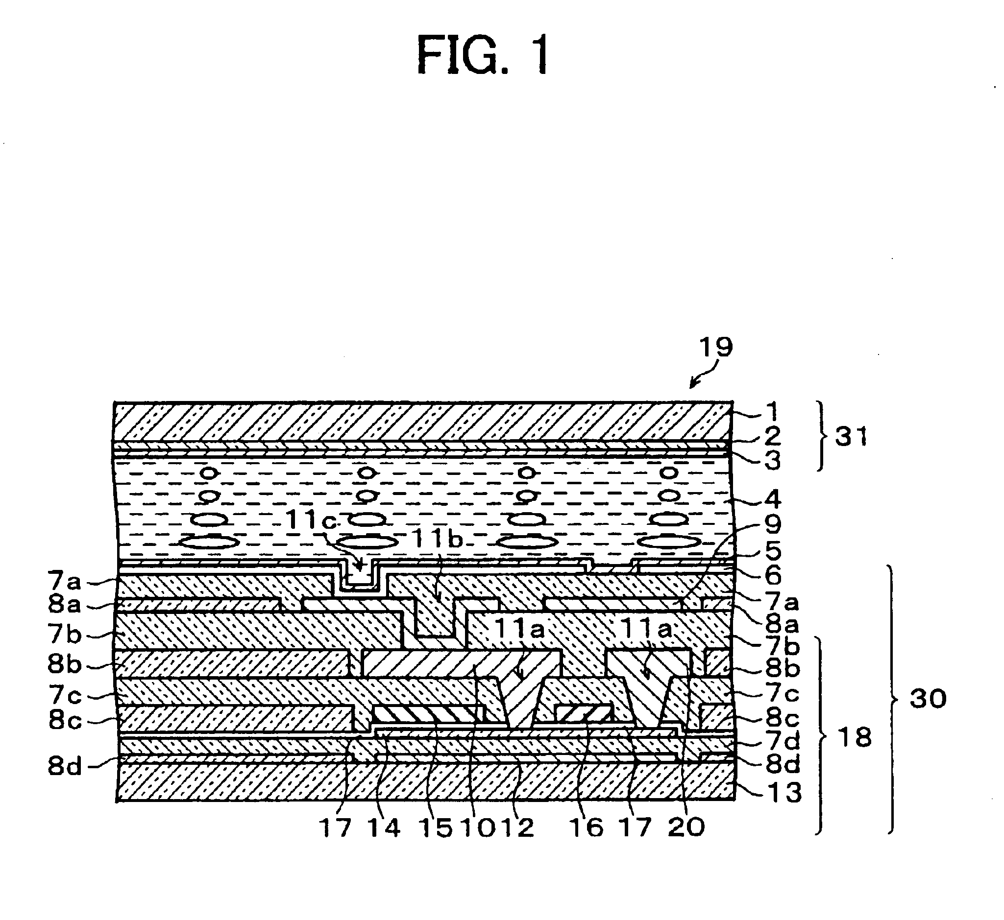
[0162]FIG. 6 shows an example case of a liquid crystal display including thin film transistors, additional capacitances, and transparent pixel electrodes provided at intersections of gate lines and signal lines crossing each other at right angles, wherein each interlayer insulating film has an insulating film pattern and is planarized by CMP.

[0163]If any one of the interlayer insulating films has no insulating film pattern in relation to manufacturing cost and productivity, that interlayer insulating film may be subjected to a conventional method, such as simple CVD whereby an insulating film is deposited.

[0164](1) A film (50 nm) of polycrystalline Si is deposited covering the entire surface of the insulating substrate 13 which is a substrate by, for example, CVD and patterned into a polycrystalline Si film 14. Next, a gate insulating film (80 nm) of SiO2 is deposited by, for example, CVD. A P-doped polycrystalline Si film (150 nm) and a WSi film (150 nm) are then sequentially depos...

example 3

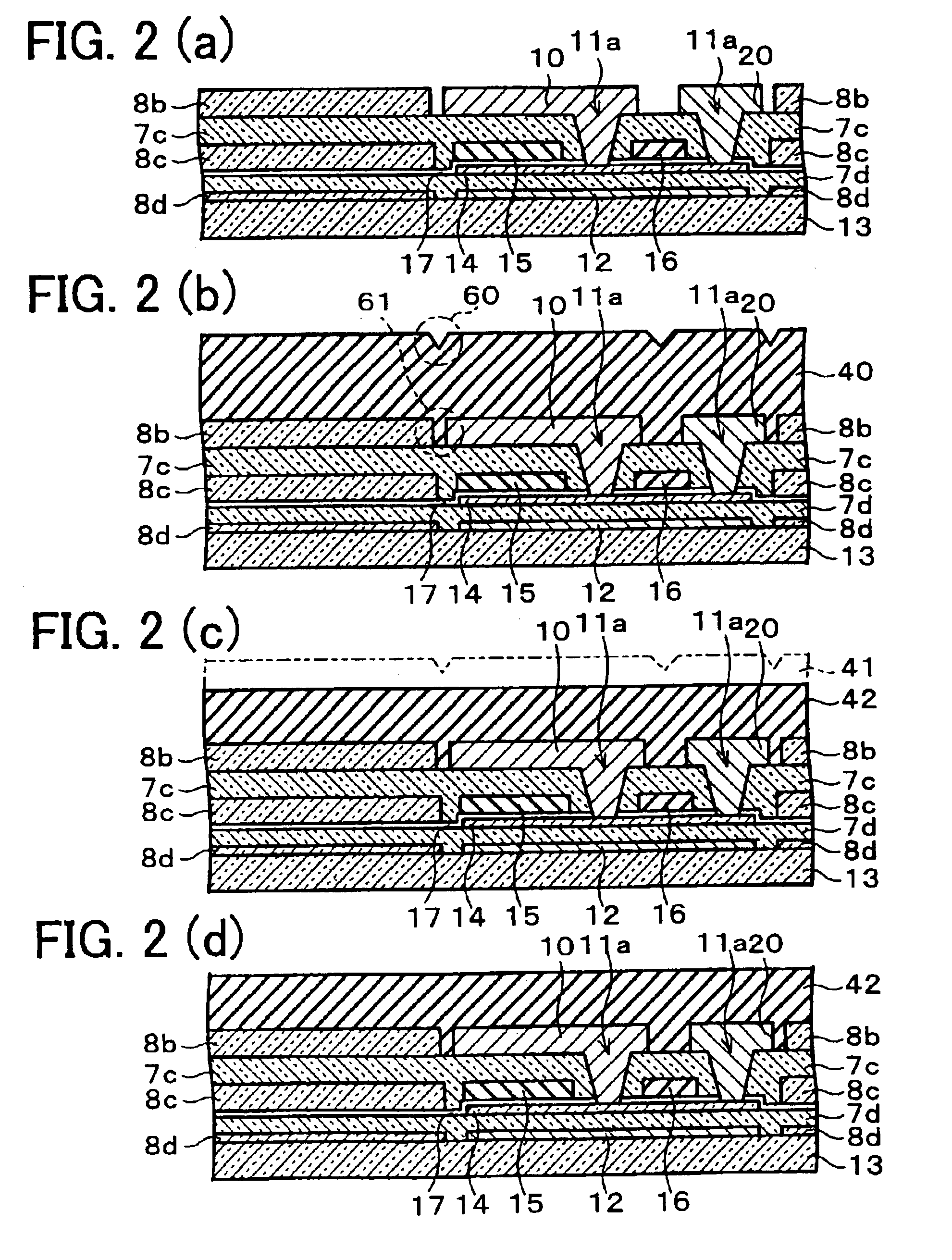
[0170]FIG. 8 shows an example case of a liquid crystal display including thin film transistors, additional capacitances, and transparent pixel electrodes provided at intersections of gate lines and signal lines crossing each other at right angles; and a first light-shield film beneath the thin film transistors with an interlayer insulating film intervening there between, wherein each interlayer insulating film has an insulating film pattern and is planarized by CMP.

[0171]If any one of the interlayer insulating films has no insulating film pattern in relation to manufacturing cost and productivity, that interlayer insulating film may be subjected to a conventional method, such as simple CVD whereby an insulating film is deposited.

[0172](1) A film (50 nm) of polycrystalline Si doped with P and a WSi film (100 nm) are sequentially deposited on an insulating substrate 13 which is a substrate and patterned into a first light-shield film pattern 12.

[0173](2) An insulating film of SiO2 is ...


PUM

PropertyMeasurementUnit
thickaaaaaaaaaa
thickaaaaaaaaaa
thicknessaaaaaaaaaa

Abstract

The invention involves: the forming of a dummy pattern for planarization between convex portions (for example, between lead electrodes and a signal wire pattern) of irregularities caused by a patterned layer on a surface on which at least one interlayer insulating film is formed, so as to be separated by a predetermined distance from the convex portions; the forming of interlayer insulating films 7a-7d so as to fill up gaps between the dummy pattern and the convex portions; and the planarizing of a surface. Thereby, the invention is capable of relaxing requirements on uniformity in the thickness of the film to be polished and the thickness of the polished portion.

Description

FIELD OF THE INVENTION[0001]The present invention relates to a substrate with a planarization film, a display substrate, and a method of manufacturing the substrates.BACKGROUND OF THE INVENTION[0002]Liquid crystal displays and like flat-panel displays have found use in a wide range of applications due to their thinness, low power consumption, and other advantages. Besides, in recent years, there are increasing demands for liquid crystal projectors as high-definition displays used in presentation, home theaters, and other situations. In many such projectors, the liquid crystal display is used as a light bulb.[0003]A typical liquid crystal display has liquid crystal sandwiched between an active matrix substrate and an opposite substrate. On the active matrix substrate are there provided signal lines and scan lines crossing each other, as well as pixel electrodes and switching devices, etc. at the respective intersections of the signal and scan lines to control the writing of a signal ...

Claims


Application Information

Patent Timeline
Patent Type & Authority Patents(United States)
IPC IPC(8): G02F1/13G02F1/1362G02F1/1333G09F9/30H01L21/304H01L21/316H01L21/3205H01L21/336H01L29/786
CPCG02F1/136227G02F1/136209G02F2001/133357G02F1/133357G02F1/1333
Inventor UEDA, TOHRU
Owner SHARP KK
Why Eureka
Try Eureka