RAM having dynamically switchable access modes

a dynamic switchable access mode and access mode technology, applied in the field of memory row decoders, can solve the problems of unpredictably changing the voltage level of bitlines, and consuming more refresh power for dram devices that require more frequent refreshing. to achieve the effect of reducing refresh power consumption and increasing data access throughput speed

Inactive Publication Date: 2005-05-17
INVENSAS CORP
View PDF12 Cites 20 Cited by
  • Summary
  • Abstract
  • Description
  • Claims
  • Application Information

AI Technical Summary

Benefits of technology

[0015]It is an object of the present invention to obviate or mitigate at least one disadvantage of the prior art. In particular, it is an object of the present invention to...

Problems solved by technology

Most systems desire fast data access speeds to achieve faster overall system performance since memory access speeds tend to bottleneck system performance.
DRAM is susceptible to soft errors caused by alpha particle bombardment for example, which can unpredictably change the voltage level of the bitlines.
Since the bitline sense amplifiers have low sensing margins to detect the few hundred milli-volt difference between the pair of complementary bitlines, alpha particle bombardment can cause misreads from the memory array.
DRAM devices that require more frequent refreshing will consume more refresh power, which is exacerbated when the DRAM operates in abnormal voltage or temperature conditions.
High power consumption due to refresh operations is undesirable, especially during a power down or sleep mode when the DRAM is not in use.
Therefore, such DRAM's are not suitable for portable applications where power is limited.
The page length of the DRAM is set by the manufacturer and thus does not necessarily meet the requirements of a specific application.
Activation of a second wordline introduces additional latency that slows the overall throughput of data.
Although DRAM manufacturers can provide devices having larger pages to accommodate these specific applications, these devices would neither be cost effective or practical for such limited applications.
Furthermore, large page mode DRAM dev...

Method used


Image

  • RAM having dynamically switchable access modes
  • RAM having dynamically switchable access modes
  • RAM having dynamically switchable access modes

Examples


case 7

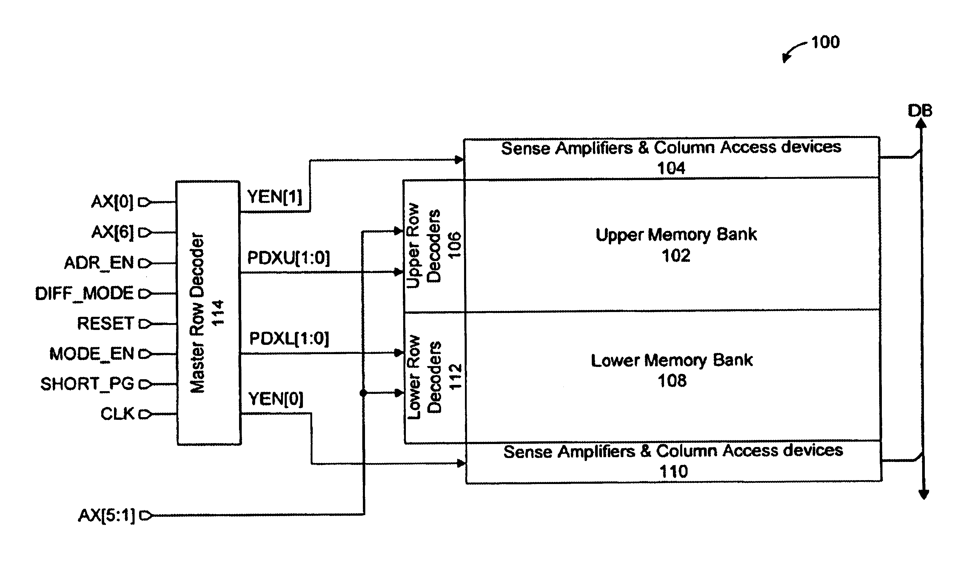
[0049 illustrates the state of master row decoder 114 when the DRAM device is set to operate in the long page access mode with two cell per bit access. More specifically, SHORT_PG is at the low logic level and DIFF_MODE is at the high logic level. Once again, because SHORT_PG is at the low logic level, address AX[6] has no effect on the outputs. However, because DIFF_MODE is at the high logic level, address AX[0] is locked out by NAND gates 210, 212, 214 and 216 and therefore has no effect on the outputs. Therefore, all the logical sub-blocks of the upper and lower row decoder blocks are enabled, as are both the bitline access circuit blocks 104 and 110. In otherwords, two wordlines in upper row decoder block 106 and two wordlines in lower row decoder block 112 are simultaneously activated.

[0050]Cases 8 and 9 illustrate the state of master row decoder 114 when the DRAM device is set to operate in the short page access mode with two cell per bit access. With DIFF_MODE at the high log...


PUM


Abstract

A row addressing circuit for DRAM memory is disclosed. Additional address or mode bits are used to dynamically select between long page and short page access modes, and to dynamically select between single cell per bit and dual, or two cell per bit modes in each memory bank within a memory block. In the short page access mode, only one wordline in a memory block is activated. In the long page access mode, two wordlines in the memory block are activated for accessing twice the number of bits as in short page access mode. In the single cell per bit mode, one bit of data is stored in one DRAM cell. In the two cell per bit mode, the row addressing circuit simultaneously activates two wordlines in a bank of the memory block to access one DRAM cell connected to each bitline of a pair of complementary bitlines for writing and reading complementary data. The row addressing circuit can combine the different access modes for system design flexibility.

Description

[0001]This application claims benefit of priority from Canadian Patent Application No. 2,342,516 filed Mar. 30, 2001 and Canadian Patent Application No. 2,342,472 flied Mar. 30, 2001, and is a continuation of U.S. Application No. 10 / 109,878, filed Apr. 1, 2002, now issued as U.S. Pat. No. 6,549,483.FIELD OF THE INVENTION[0002]The present invention relates to semiconductor memories. In particular the invention relates to memory row decoders.BACKGROUND OF THE INVENTION[0003]DRAM memory cells consist of a single transistor and storage capacitor, where the storage capacitor can be formed as a planar, trench or stacked capacitor. DRAM memories are generally accessed by supplying a row address and a column address to access memory cells within the memory array. More specifically, the row address activates a selected wordline and the column address enables data to be transferred between selected complementary bitline pairs and a databus. The following description briefly highlights how mem...

Claims


Application Information

Patent Timeline
IPC IPC(8): G11C7/00G11C8/00
CPCG11C7/1045G11C11/4087G11C11/408G11C11/4076
Inventor KURJANOWICZ, WLODEKWIATROWSKI, JACEKKOWALCZYK, DARIUSZPOPOFF, GREG
Owner INVENSAS CORP
Why Eureka
Try Eureka