Reducing chromatic aberration in images formed by emmission electrons

Inactive Publication Date: 2005-05-24
NAT UNIV OF SINGAPORE
View PDF1 Cites 5 Cited by
  • Summary
  • Abstract
  • Description
  • Claims
  • Application Information

AI Technical Summary

Benefits of technology

[0011]In accordance with an aspect of the present invention, an imaging device, such as an EEM, includes an electric/magnetic lens is used to focus pulsed electrons emitted from an object on to a target plane. Before a pulse of emitted electrons reaches the lens, electrons are spatially separated in dependence on their respective kinetic energies and are then subject to a time varying electric field. The electric field compensates for varia

Problems solved by technology

Not focusing a beam in a single plane results in distortion of the image formed on a single plane.
Thus, the spatial resolution of electric/magnetic lenses is limited in part by chromatic aberration.
Further, certain information is lost.
Particularly, a full emission spectrum cannot be o

Method used


Image

  • Reducing chromatic aberration in images formed by emmission electrons
  • Reducing chromatic aberration in images formed by emmission electrons
  • Reducing chromatic aberration in images formed by emmission electrons

Examples


Embodiment Construction

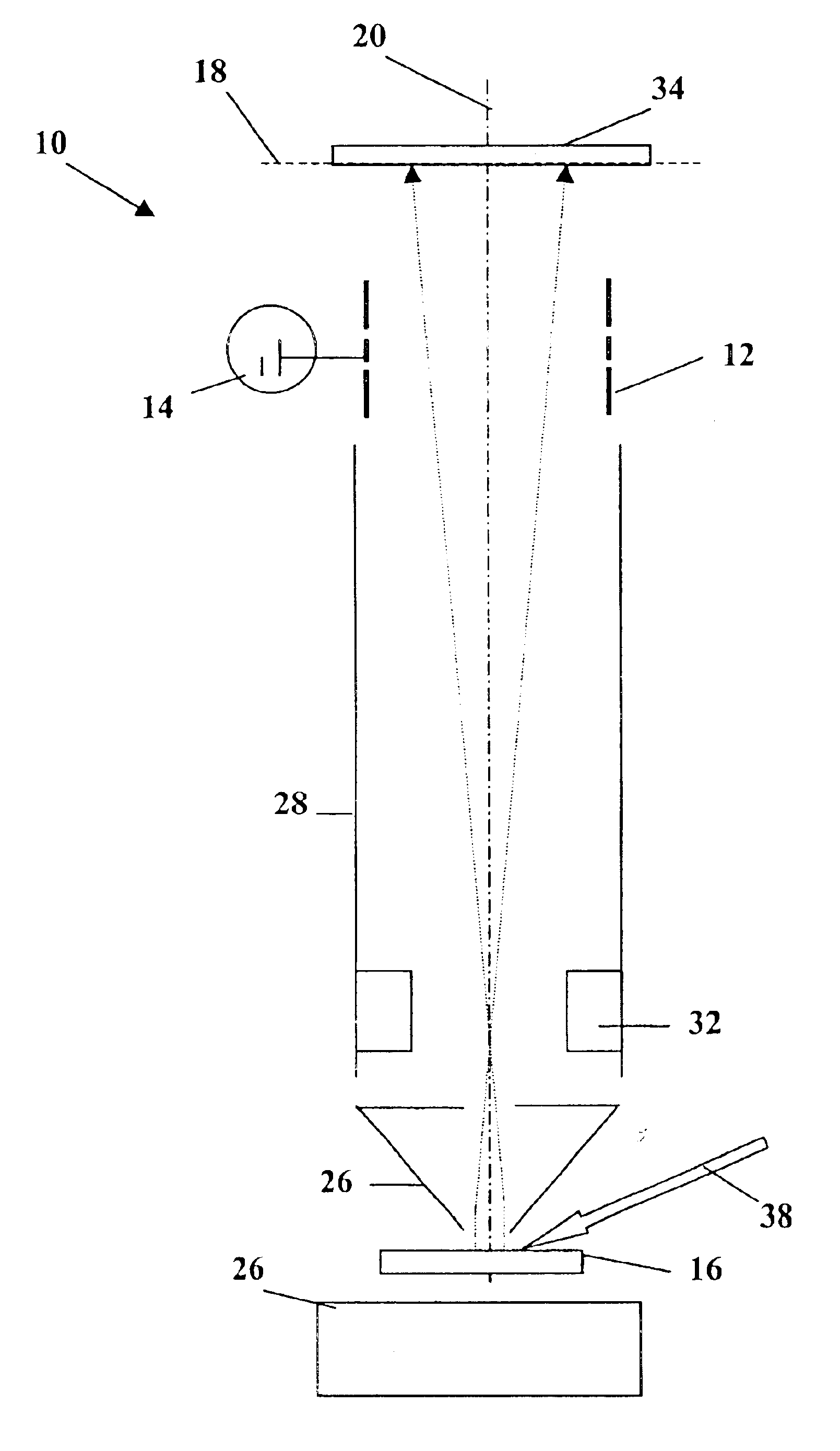
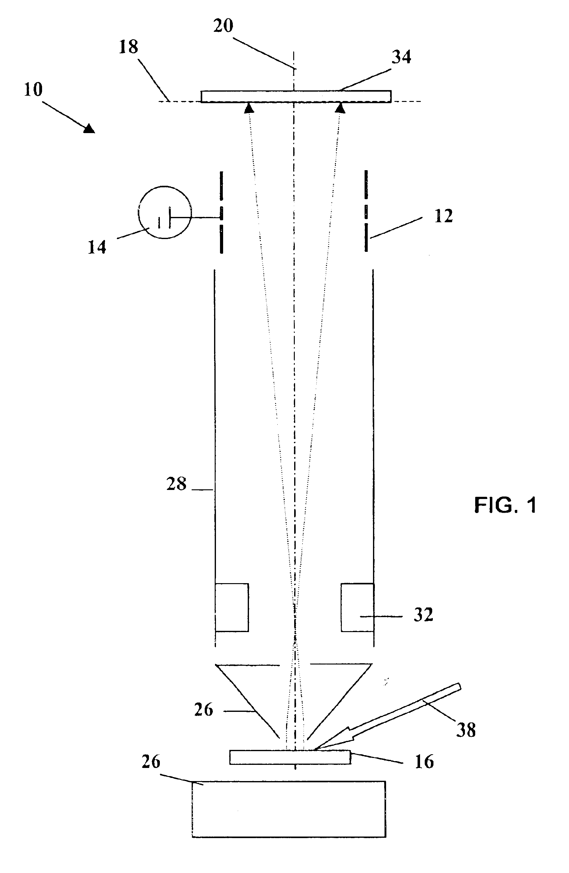
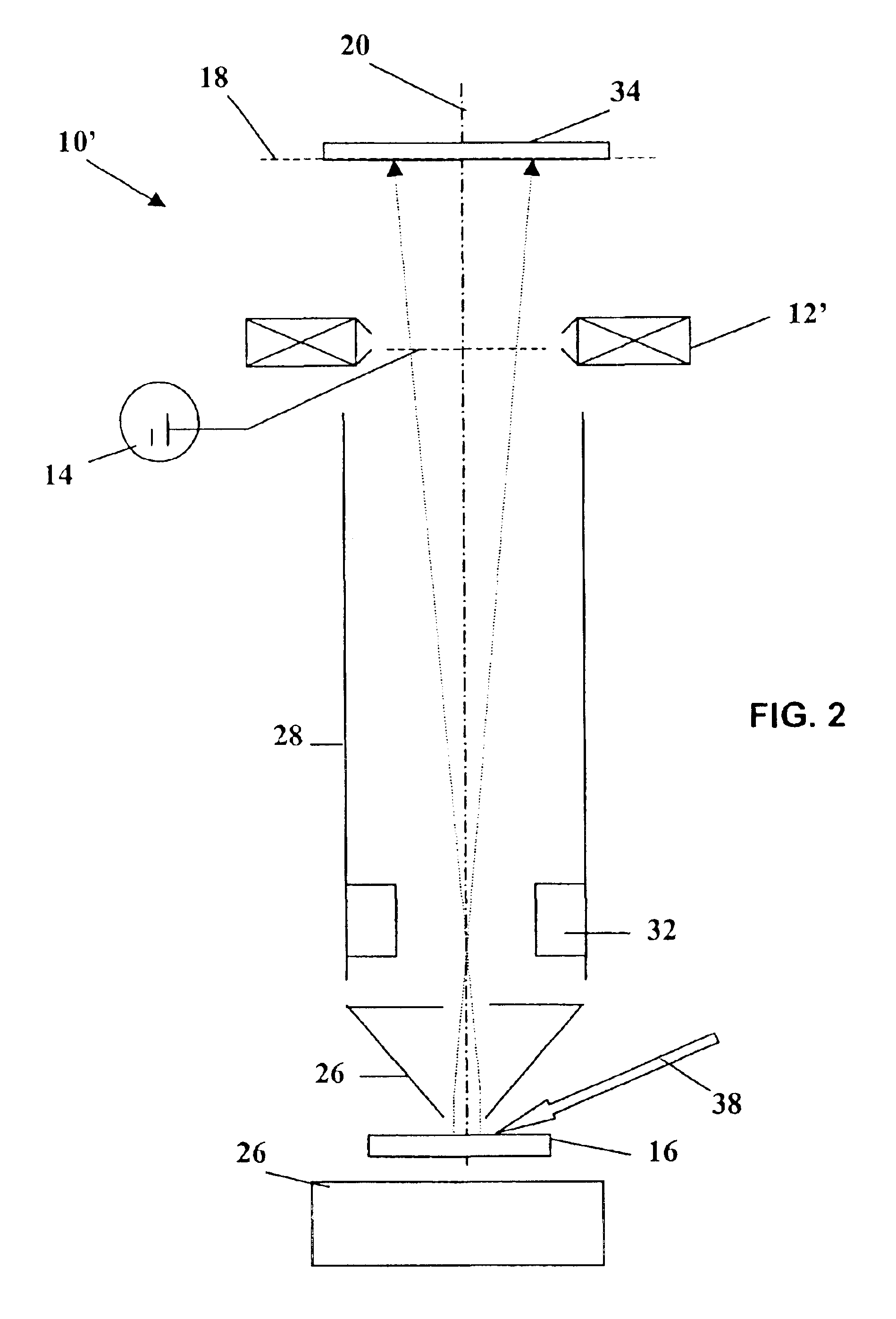
[0023]FIG. 1 illustrates an EEM 10, exemplary of an embodiment of the present invention. EEM 10 includes an objective lens 26, a drift chamber 28, a dynamic projector lens 12, and an electron detector 34. An optional deflector / stigmator unit 32 also forms part of EEM 10. EEM 10 may be used to image an object 16 or a portion thereof using pulsed electrons emitted from object 16. Beam 38 may be a beam of electromagnetic waves, such as UV light or X-rays, or charged particles, such as electrons. A radiation source (not shown) may form part of EEM 10 to excite object 16 to emit electrons by generating radiation beam 38. Drift chamber 28 may have an axial length between 20 and 100 cm. An example detector 34 may include a multi-channel-plate (MCP) and a digital sampling oscilloscope to image object 16.

[0024]Lens 12 is positioned at a distance from object 16 to focus electrons emitted from object 16 in a target plane 18 along an optical axis 20 to form an image 22 of object 16.

[0025]An ele...


PUM


Abstract

An imaging device, such as an EEM, includes an electric/magnetic lens used to focus pulsed electrons emitted from an object on to a target plane. Before a pulse of emitted electrons reaches the lens, electrons are spatially separated in dependence on their respective kinetic energies and are then subject to a time varying electric field that keeps the final focal plane constant for a wide variety of different energy electrons. The electric field compensates for variations in the image focal length caused by a spread in kinetic energies, causing the electrons to be focused proximate the target plane, reducing chromatic aberration. The varying electric field may be provided by varying an electric potential at the lens by, for example, varying a voltage supplied to an electrode at the lens. This potential effectively varies the focal strength of the lens in time, in order to compensate for variations in kinetic energies of electrons arriving at the lens, effectively keeping the image plane position constant.

Description

CROSS REFERENCE TO RELATED APPLICATIONS[0001]This application claims priority from U.S. provisional patent application Ser. No. 60 / 393,133 which is entitled “Low Voltage Time of Flight Electron Emission Microscope,” filed Jul. 3, 2002, and is hereby incorporated herein by reference.FIELD OF THE INVENTION[0002]The present invention relates to imaging objects with emission electrons.BACKGROUND OF THE INVENTION[0003]Many modern electrical imaging devices, such as modern electron emission microscopes (EEMs), image an object of interest (also called specimen or sample) by first accelerating and focusing electrons emitted from the object using an electric / magnetic objective lens, and then further magnifying the image by using a series of electric / magnetic projector lenses. An electric / magnetic lens typically generates electric or magnetic fields, or a mix of both, in the path of a beam of emitted electrons for altering the trajectories of the emitted electrons, analogous to the way a glas...

Claims


Application Information

Patent Timeline
IPC IPC(8): H01J37/285H01J37/153H01J37/04H01J37/26G01Q30/02
CPCH01J37/285H01J37/153
Inventor KHURSHEED, ANJAM
Owner NAT UNIV OF SINGAPORE
Why Eureka
Try Eureka