Twin insulator charge storage device operation and its fabrication method

a charge storage device and twin insulator technology, applied in semiconductor devices, instruments, electrical devices, etc., can solve the problems of limited hot hole and che combination approach, and achieve the effect of high density nand and easy integration into a conventional cmos platform

Active Publication Date: 2005-05-31
HALO LSI INC
View PDF10 Cites 34 Cited by
  • Summary
  • Abstract
  • Description
  • Claims
  • Application Information

AI Technical Summary

Benefits of technology

[0018]The fourth embodiment is for higher density NAND application using MONOS memory. The memory cell structure consists of subtracting the word gate from the third embodiment. It is simply replacing the polysilicon floating gate of the conventional NAND cell by nitride. The unit cell along the channel direction consists of a half of source / drain, a control gate with underlying ONO as an memory storage and other half of source / drain. The width of the control gate and underlying ONO is defined by an overlying oxide sidewall mask. The unit cell dimension along the channel can be smaller than the conventional NAND. The direction across the channel is bounded by STI along the channel. The array structure follows NAND only replacing the floating gate by nitride. The bit lines run along the active area isolated by STI lines. The control gate lines are across the bit lines. A block consists of every a certain number of the control gate lines and bit lines. The control gates at both ends of the block are utilized as select gates to define which block is operated. The diffusion area in between the blocks is shared as a bit diffusion connected to a bit line through contact and common ground, alternately. The control gate mask on a sidewall is looped. The looped mask is separated into two lines by cutting it at both ends. The control gate contact is also placed at the ends.
[0019]The device operation method of the fourth embodiment is designated by F-N program and F-N erase through the top oxide. This is different from the conventional NAND operation access through the tunnel oxide. Even in F-N ejection through the bottom oxide, a small number of hot holes are generated by band to band transition and accumulated at the channel surface. The hot holes are easily injected through the bottom oxide and leave damage in the bottom oxide. This degrades the retention time after program-erase cycles. On the other band, F-N tunneling through the top oxide may not have a concern about such hot hole generation. The F-N tunneling through the top oxide is considered to be more reliable than tunneling through the bottom oxide. Two device operation methods using F-N tunneling through the top oxide are provided as program / erase defined by electron ejection / injection and injection / ejection.
[0020]Multi level program method is also contained in the device operation methods. Multi level program is to provide controllable memory cell threshold voltage Vt at 4 or 8 levels by adjusting operation conditions. A memory cell with 4 level Vt is a two-bit cell so that the density of the two bit cell memory array becomes twice that of the single bit cell memory array. The multi level Vt program is allowed by adjusting the control gate voltage or bit line voltage.
[0021]The fabrication method of the fourth embodiment is designated by skipping the word gate polysilicon in the third embodiment. The process steps through to sidewall oxide mask are the same as in the third embodiment. Stripping the cap nitride, only the looped oxide mask remains on the control gate polysilicon. The loop is cut at both ends of a block into two lines. A photoresist mask for the control gate contact cover and logic gate is printed on the polysilicon. The polysilicon is vertically etched out with the sidewall oxide mask and the photoresist mask, followed by clearing ONO. The device impurity profile is defined by a LDD implant, spacer process, and source-drain implant. After oxide deposition and planarization, the common source line and bit contact are formed by a damascene process.
[0022]The fifth embodiment in this invention is for NOR application using the same cell structure and fabrication method as the fourth embodiment. The control gate having ONO storage runs across STI (active area). The bit line crosses the control gate. The diffusion area is formed on the active area at both sides of the control gate. The diffusion area on one side is connected to bit line through the bit contact. The diffusion areas on the other side are connected together as a common source line. An individual memory cell is addressed by selecting a bit line and control gate.
[0023]The sixth embodiment is a single gate MONOS. The cell structure is of simply replacing the gate oxide of a conventional MOS FET by ONO. The memory cell can have dual memory storage in nitride over the p-n junction. The memory cell structure is close to NROM proposed by B. Eitan et al, SSDM 1999. Proc, p. 522, but it is different in using a metal bit line instead of a diffusion bit line and STI instead of field implant isolation. The memory cell can be fabricated with only one extra mask compared to a conventional CMOS device. The memory cell is easily embedded into a conventional CMOS platform. The array structure is derived from Twin MONOS metal bit application. The control gate and underlying ONO run crossing the STI and active area. The bit line also crosses the control gate. Every other diffusion area bounded by the STI and the control gate is connected to the bit line through a contact. Program operation adapts electron injection into the nitride with channel hot electron to store the electrons on each side independently. Erase operation is either with hot hole injection or F-N ejection. There arises a concern about enduring the program-erase cycles. The difference of mean free path between an electron and a hole causes mismatch of their injection profile along the channel. A few electrons remain at the middle of the channel without being neutralized by hot holes. These electrons are accumulated with the program-erase cycle so that threshold voltage is going up. It is a common concern with NROM. It is disclosed to inject hot holes from not only one side but also the other side of the channel.

Problems solved by technology

However, this Hot Hole and CHE combination approach is still limited by Hot Hole endurance comparing to CHE-F-N endurance.

Method used


Image

  • Twin insulator charge storage device operation and its fabrication method
  • Twin insulator charge storage device operation and its fabrication method
  • Twin insulator charge storage device operation and its fabrication method

Examples


first embodiment

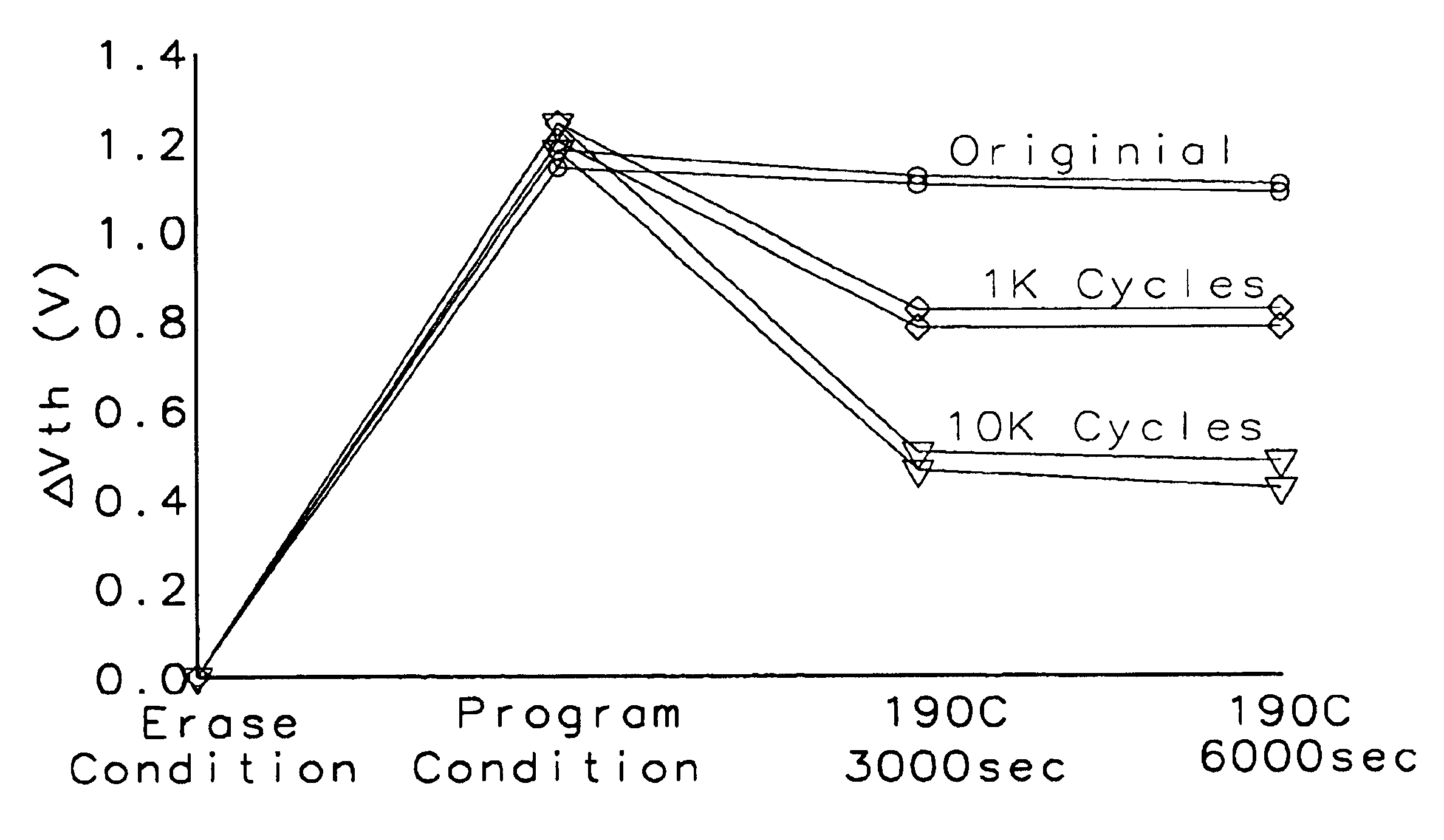
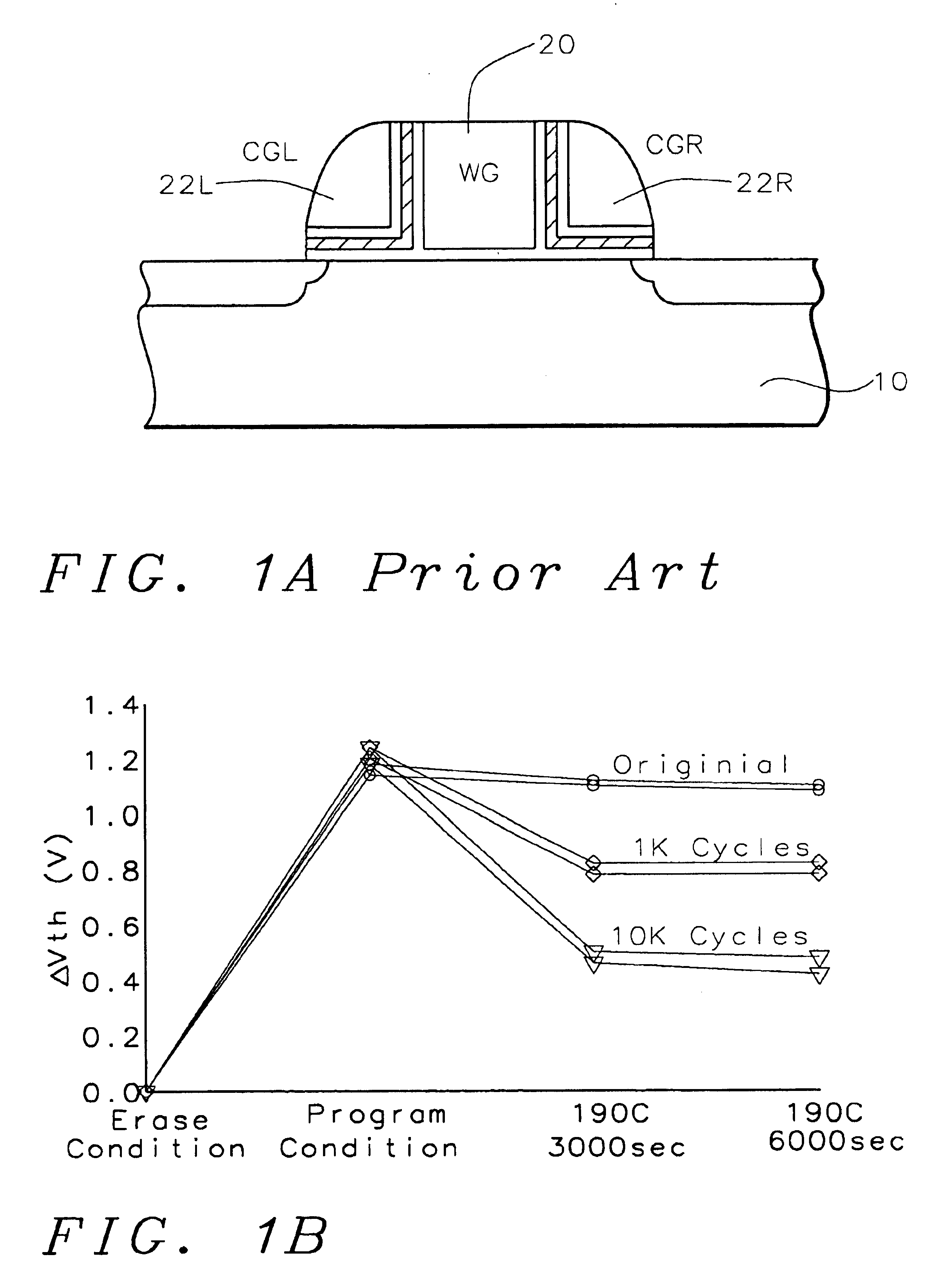
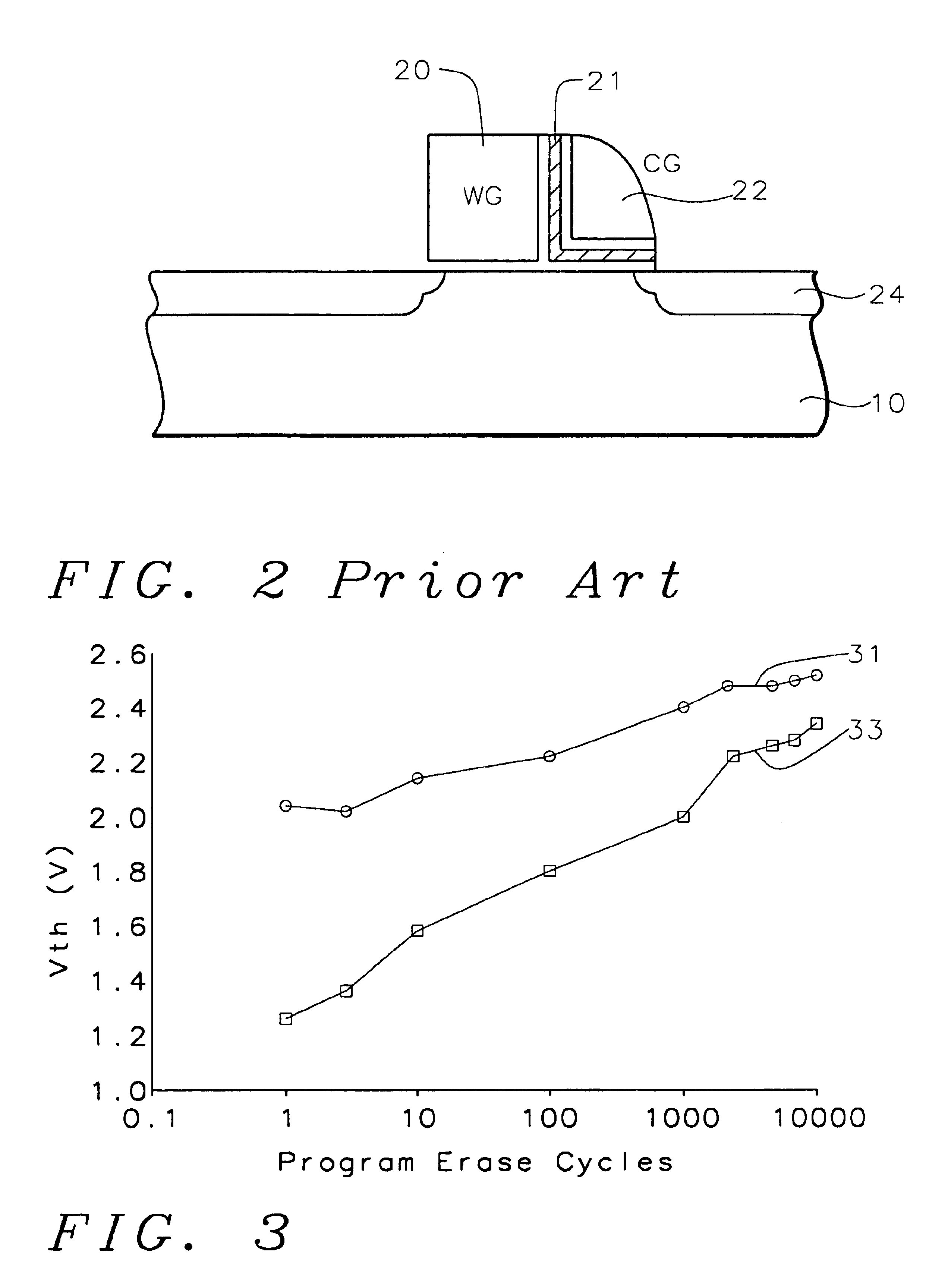
[0057]It is implemented for device operation of the first embodiment to insert one hot hole erasure after every n (100 or 1000) cycles of CHE program and F-N erase as shown in FIG. 6. Hot holes generated by band to band transition can be injected into the nitride portion at the L-shaped corner and neutralize the accumulated electrons there as long as the control gate (CG) channel length is within the several hole mean free path by applying a negative bias on the word gate. (See U.S. patent application Ser. No. 09 / 810,122—Halo 00-004—Word gate negative hole injection). Therefore if hot hole damage is tolerable up to 1K cycles and hot hole injection is required after 100 F-N erasures, then the endurance cycle providing the proper operating threshold voltage (Vt) window is extended to 100×1K=100K cycles. However, this Hot Hole and CHE combination approach is still limited by Hot Hole endurance comparing to CHE-F-N endurance.

second embodiment

[0058]The device cross-sectional structure of the second embodiment along the 1′ direction is shown in FIG. 7 as well as the top view of array architecture shown in FIG. 8. The bit diffusion is in between a pair of the control gates partitioned by memory spacer 115. The bit diffusion consists of memory diffusion 103 and overlying raised diffusion 141. The control gate consists of the control gate polysilicon 140, underlying ONO (bottom oxide 111, storage nitride 112 and top oxide 113) and underlying control gate channel 101. The pair of the control gates are connected to each other at the end of diffusion bit. The control gate and the bit diffusion run along the 2nd direction crossing the 1st direction. Their contacts are placed at the end of the bit diffusion. The word gate consisting of word gate polysilicon 142, underlying word gate oxide 118 and underlying substrate 100 is on the other side of the control gate partitioned by CG-WG isolation dielectrics 118. The word gates are co...

third embodiment

[0090]Referring to FIGS. 29A, B, C and C1, FIG. 29C is a cross section along word gate polysilicon 240 (cross-section G-G′) and FIG. 29C1 is along the word gate space (cross-section F-F′). After oxide planarization, adjacent every pair of diffusions are connected together by local wiring 250 as shown in FIG. 29C1. The bit contact 251 is paced on the center of the local wiring 250. The bit contacts are connected by the 1st metal 252. The control gate contact 260 and the word contact 261 are placed at the end of the word line as shown in FIGS. 29A and C. The third embodiment is therefore completed.

[0091]A top view and a cross sectional structure of the fourth embodiment are shown in FIG. 30A and FIG. 30B. It is simply replacing the floating gate in the conventional NAND by nitride 312 besides reducing the cell size. The memory cell structure is of subtracting the word gate 242 in FIG. 23B of the third embodiment and forming a diffusion area instead. The unit cell is shown in FIG. 30 a...


PUM


Abstract

The invention proposes am improved twin MONOS memory device and its fabrication. The ONO layer is self-aligned to the control gate horizontally. The vertical insulator between the control gate and the word gate does not include a nitride layer. This prevents the problem of electron trapping. The device can be fabricated to pull the electrons out through either the top or the bottom oxide layer of the ONO insulator. The device also incorporates a raised memory bit diffusion between the control gates to reduce bit resistance. The twin MONOS memory array can be embedded into a standard CMOS circuit by the process of the present invention.

Description

[0001]This application claims priority to U.S. Provisional Patent Applications Ser. No. 60 / 418,451 filed on Oct. 15, 2002 now abandoned and Ser. No. 60 / 436,129 filed on Dec. 23, 2002, which are herein incorporated by reference.BACKGROUND OF THE INVENTION[0002](1) Field of the Invention[0003]The Invention relates to a high-density non-volatile memory device using Twin-MONOS structure, and its fabrication method.[0004](2) Description of the Prior Art[0005]An insulator charge storage device is a type of non-volatile memory in which charge is stored within the traps of an insulator material. Electrons may be injected into the insulator by either channel hot electron (CHE) or tunneling. Electrons are usually eliminated via some type of hole injection mechanism in a MONOS device contrasting to FN ejection in a floating gate silicon device. In a MONOS device, nitride is the storage element. When the bottom oxide is as thin as or less than 23 Angstroms, holes are injected by a direct tunnel...

Claims


Application Information

Patent Timeline
Patent Type & Authority Patents(United States)
IPC IPC(8): H01L21/02H01L21/336G11C16/04H01L21/28H01L21/8246H01L27/105H01L27/115H01L29/02H01L29/423H01L29/792H01L47/00
CPCG11C16/0466G11C16/0475H01L21/28282H01L27/105H01L27/115H01L27/11568H01L29/4234H01L29/42364H01L29/66833H01L29/792H01L29/7923H01L2924/0002G11C16/0483H01L2924/00H01L29/40117H10B69/00H10B43/30
Inventor OGURA, SEIKISATOH, KIMIHIROSAITO, TOMOYA
Owner HALO LSI INC
Why Eureka
Try Eureka