Focused ion beam system with coaxial scanning electron microscope

a coaxial scanning electron microscope and focused ion beam technology, applied in the field of electron beam imaging and micromachining microscopic features, can solve the problems of sample damage during the fib image process, the limit on the size of the write head that can be manufactured using lithographic techniques alone, and the placement accuracy of the fib beam to the sem image has limitations, so as to achieve superior and non-destructive sem imaging

Inactive Publication Date: 2005-05-31
FEI CO
View PDF9 Cites 77 Cited by
  • Summary
  • Abstract
  • Description
  • Claims
  • Application Information

AI Technical Summary

Benefits of technology

[0029]An object of the invention, therefore, is to combine the micromachining capabilities of a FIB system and the superior and non-destructive imaging of a SEM in an instrument suitable for high-accuracy mass production of nanodevices. A preferred embodiment of the invention described and claimed herein comprises a combination FIB and SEM sharing a final electrostatic lens and having a common axis as the beams approach the work piece.

Problems solved by technology

When the FIB beam is employed to form an image of the work piece to align the beam for milling, sample damage may result by exposing sensitive regions to the high-energy ion beam.
In either case, the placement accuracy of the FIB beam to the SEM image has limitations due to stage inaccuracies, sample non-flatness, and—in the case of coincident beams—the different beam angles.
However, there is a limit on how small a write head can be manufactured using lithographic techniques alone.
Unfortunately, thin film head trimming and other nanofabrication applications may suffer from sample damage during the FIB image processes.
If the FIB beam image time is reduced to decrease sample damage, the image signal-to-noise ratio may be insufficient for accurate milling placement.
In other cases, it may be undesirable to ever direct the FIB beam at certain sensitive structures.
However, the momentum of an electron in a typical SEM electron beam is not sufficient to remove molecules from a surface by momentum transfer.
Although an SEM beam is typically much less destructive than an ion beam, certain work pieces, such as some integrated circuits, are susceptible to damage by higher energy electron beams.
Minor differences in the distances between final lens of each system and the work piece affect the relative positions of the two beams, so there is always misalignment when switching between the beams.
Some sample displacement is inevitably caused during stage tilt.
In addition, if the detector is on the side, image shadowing will result, which is sometimes undesirable.
While coaxial column FIB-SEM systems have been described in the literature, all such systems existing to date suffer from design characteristics that limit their usefulness for high-precision or mass production applications.
As a result, the beams cannot operate simultaneously.
When a lens is switched on, a period of time is required for the lens to stabilize, making such a system unsuitable for a high throughput production environment.
Also, magnetic lenses have hysteresis effects, which inhibit accurate beam placement after shutting the lens off.
Although this system does allow simultaneous use of the beams, the use of lenses in series results in an increase in focal length, which typically degrades the resolution of the FIB system.
This also requires an increased focal length and limits secondary electron collection efficiency and accuracy when using through-the-lens detection of secondary electrons (discussed in greater detail below).
As a result, the design of the Sawaragi II patent does not provide the resolution required for advanced thin film head trimming and other nanofabrication applications.
Smaller systems are desirable because many systems are located in a clean room, and the cost of clean room space is extremely high.
Finally, the combination lens system used by the Sawaragi II patent is more complex than a single lens system.
This tends to reduce the reliability of such a system and make it less suitable for mass production manufacturing.
However, the system described in Cleaver uses an einzel lens—a unipotential electrostatic lens—to focus both the ion and electron beams.
The Cleaver system does not provide the flexibility to readily adjust the beam voltage for different applications.
A large voltage change in the final lens can take as much as one second—a significant amount of time in the mass production process.

Method used


Image

  • Focused ion beam system with coaxial scanning electron microscope
  • Focused ion beam system with coaxial scanning electron microscope
  • Focused ion beam system with coaxial scanning electron microscope

Examples


Embodiment Construction

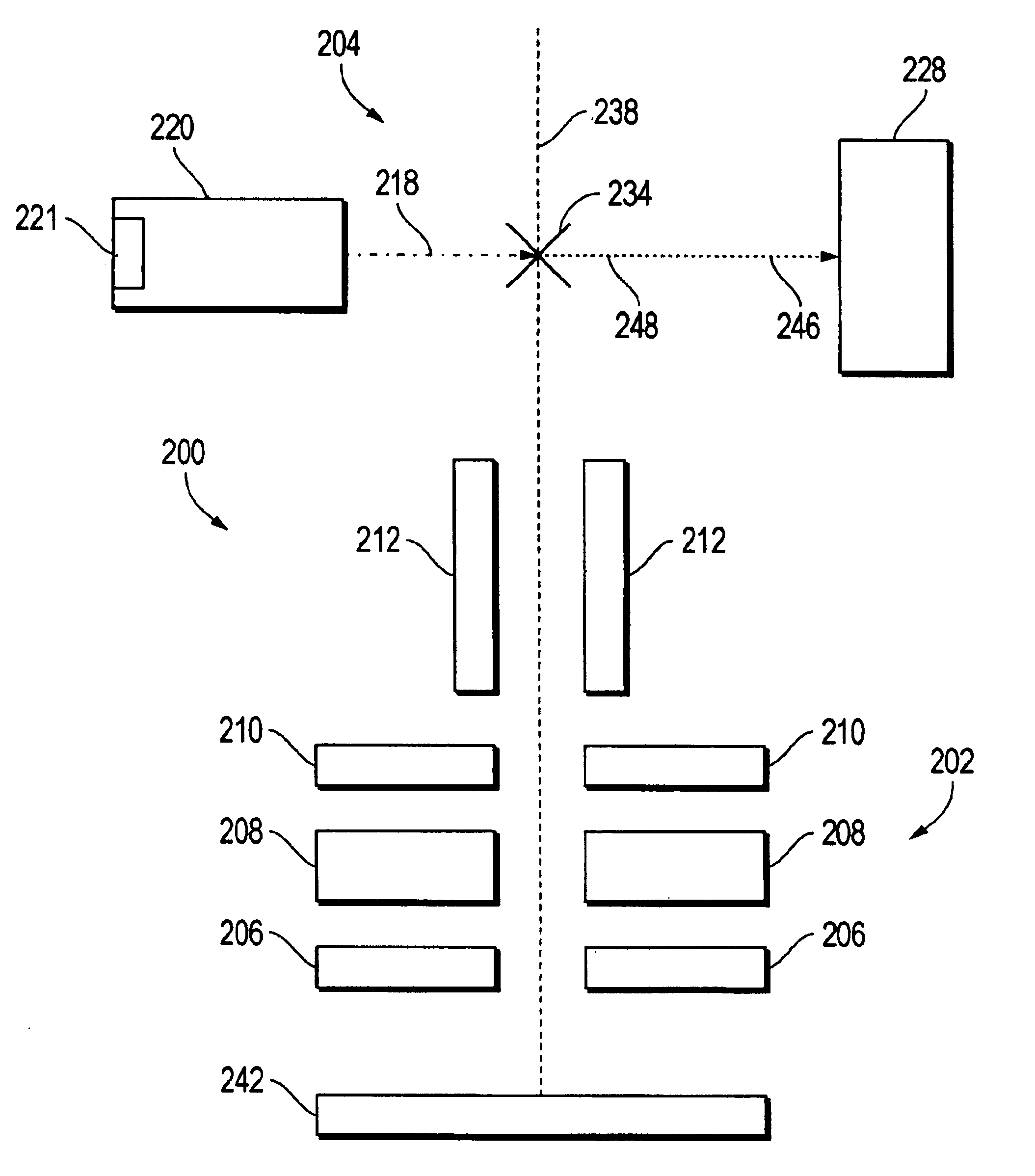
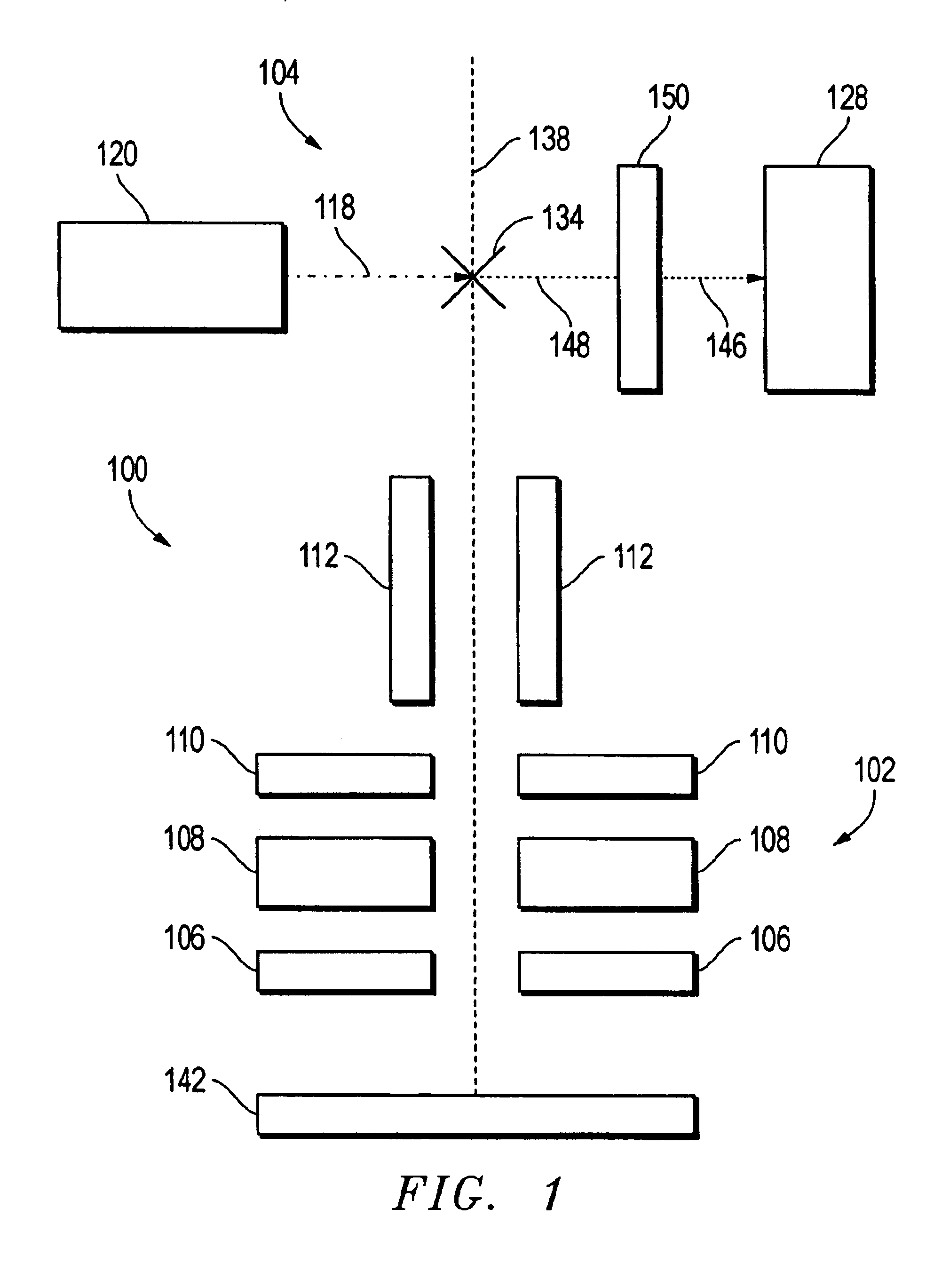
[0049]The embodiments described below accomplish several different design goals for a FIB-SEM device sharing a final lens and having both beams approximately coaxial as they approach the work piece. The SEM alignment of FIB milling is accurate enough to allow processing such as manufacturing, modification, sample preparation, or metrology of various nanodevices, and it avoids the sample damage that results from FIB imaging. Optional through-the-lens detection of secondary electrons allows the sample to be placed close to the final lens, thus shortening the working distance and improving performance.

[0050]Throughput will be improved since the final lens high voltage need not be adjusted when changing beams. Mass production—including modification, sample preparation, and metrology—requires that any necessary micromachining be done very rapidly. A large voltage change in the final lens can take as much as 1 second—a significant amount of time in the mass production process. Therefore, ...


PUM

PropertyMeasurementUnit
voltageaaaaaaaaaa
voltageaaaaaaaaaa
voltageaaaaaaaaaa

Abstract

A system including co-axial focused ion beam and an electron beam allows for accurate processing with the FIB using images formed by the electron beam. In one embodiment, a deflector deflects the electron beam onto the axis of the ion beam and deflects secondary particles collected through the final lens toward a detector. In one embodiment, a positively biased final electrostatic lens focuses both beams using the same voltage to allow simultaneous or alternating FIB and SEM operation. In one embodiment, the landing energy of the electrons can be varied without changing the working distance.

Description

[0001]This application claims priority from U.S. Provisional Pat. App. 60 / 401,718, filed Aug. 7, 2002, which is hereby incorporated by reference.TECHNICAL FIELD OF THE INVENTION[0002]The present invention relates to the fields of electron beam imaging and micromachining microscopic features using charged particle beams.BACKGROUND OF THE INVENTION[0003]Various nanofabrication, lithography, sample preparation, metrology, or inspection applications of focused ion beam (FIB) systems require very accurate placement of the FIB milling beam (on a nanometer scale). When the FIB beam is employed to form an image of the work piece to align the beam for milling, sample damage may result by exposing sensitive regions to the high-energy ion beam.[0004]Dual beam systems, including a FIB and a scanning electron microscope (SEM), have been introduced which can image the sample with the SEM and mill on the sample using the FIB. Some dual beam instruments utilize coincident FIB and SEM beams, where t...

Claims


Application Information

Patent Timeline
Patent Type & Authority Patents(United States)
IPC IPC(8): G01N23/00G21K7/00H01J37/12H01J37/10H01J37/26H01J37/05H01J37/244H01J37/28H01J37/305H01J37/317
CPCH01J37/12H01J37/28H01J37/3056H01J2237/31749H01J2237/31732H01J2237/3174H01J2237/12
Inventor GERLACH, ROBERT L.UTLAUT, MARK W.SCHEINFEIN, MICHAEL R.
Owner FEI CO
Why Eureka
Try Eureka