

Semiconductor device and manufacturing method thereof
- Summary
- Abstract
- Description
- Claims
- Application Information
AI Technical Summary
Benefits of technology
Problems solved by technology
Method used
Image

Examples
experiment 1
(Experiment 1)
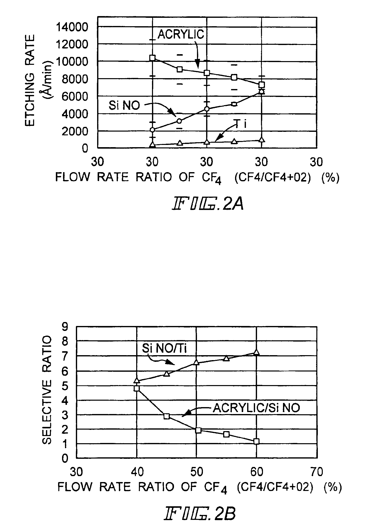
[0066]An experiment was conducted by first changing the flow rate ratio of CF4 to oxygen in dry etching. Setting 400 W (2.56 W / cm2) to an RF electric power, 0.4 Torr to a gas pressure, 35 sccm to an He flow rate, and 40 sccm / 60 sccm, 45 sccm / 55 sccm, 50 sccm / 50 sccm, 55 sccm / 45 sccm, and 60 sccm / 40 sccm to a CF4 flow rate / oxygen flow rate, respectively, the experiment was conducted.
[0067]The result of this experiment is shown in FIGS. 2A and 2B. When the flow rate ratio of CF4 is increased, the etching rate of acrylic resin film with respect to the etching gas decreases whereas the etching rate of silicon oxide nitride film with respect to etching gas increases as shown in FIG. 2A. The graph of FIG. 2B illustrating a selective ratio (etching rate of acrylic resin film / etching rate of silicon oxide nitride film, etching rate of silicon oxide nitride film / etching rate of Ti film) is based on FIG. 2A.
[0068]Furthermore, photographic views that correspond to the respective ...
experiment 2
(Experiment 2)
[0073]The next experiment was conducted by setting the flow rate ratio of CF4 to oxygen in dry etching at 50 / 50 and changing the gas pressure. Setting 400 W (2.56 W / cm2) to the RF electric power, 35 sccm to the He flow rate, and 0.2 Torr, 0.3 Torr, 0.4 Torr, and 0.5 Torr to gas pressure, respectively, the experiment was conducted.
[0074]The result of this experiment is shown in FIGS. 6A and 6B. FIG. 6A is a graph illustrating a pressure dependency of the etching rate and FIG. 6B is a graph illustrating a pressure dependency of the selective ratio. By lowering the pressure in this experiment, the overhang in the top portion of the contact hole can be suppressed.
experiment 3
(Experiment 3)
[0075]Next, another experiment was conducted by setting the flow rate ratio of CF4 to oxygen in dry etching at 50 / 50 and changing the RF electric power. Setting 0.4 Torr to gas pressure, 35 sccm to the He flow rate, and 300 W, 400 W, 500 W, and 600 W to the RF electric power, respectively, the experiment was conducted.
[0076]The result of this experiment is shown in FIGS. 7A and 7B. FIG. 7A is a graph illustrating an RF electric power dependency of the etching rate and FIG. 7B is a graph illustrating an RF electric power dependency of the selective ratio. By making the RF electric power higher, the overhang in the top portion of the contact hole can be suppressed.
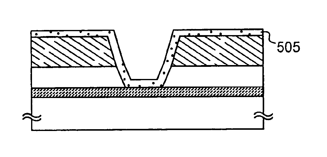
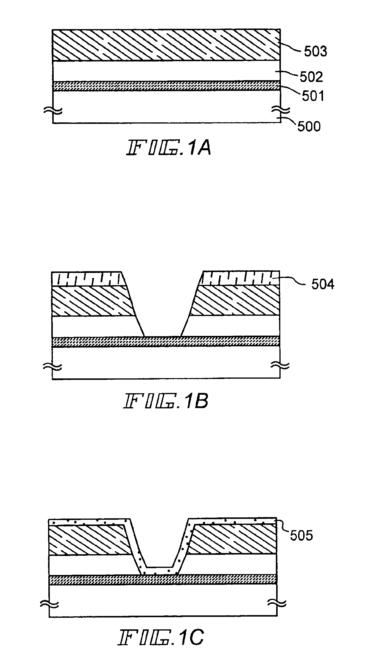
[0077]By employing one condition (the flow rate ratio of CF4 to oxygen to He at 50 / 50 / 35, gas pressure at 0.3 Torr, RF electric power at 400 W) from among the preferable range that can be obtained from the results of experiments 1 to 3, the contact hole is opened taper shaped in multiple steps and a desirable s...
PUM
 Abstract
Description
Claims
Application Information