Method and system for controlling the processing of an integrated circuit chip assembly line using a central computer system and a common communication protocol

a technology of integrated circuit chip and computer system, which is applied in the field of backend manufacturing of ic packaged chips, can solve the problems of high level of work-in-progress (wip) inventory, relatively high cycle time, and inability of factory management to meet the needs of manufacturing, and achieve the effect of increasing the throughput time of a specific package size and increasing the flexibility of the package family

Inactive Publication Date: 2005-06-07
MONTEREY RES LLC
View PDF2 Cites 7 Cited by
  • Summary
  • Abstract
  • Description
  • Claims
  • Application Information

AI Technical Summary

Benefits of technology

[0023]In one embodiment, the various substations of the integrated in-line back-end IC manufacturing hardware are arranged in an assembly line format. Further, a software process monitors and controls the integrated in-line back-end IC manufacturing hardware. It is also appreciated that an automated reject management protocol is implemented from initial die attach through test and finish. Specifically, the reject management protocol maintains a strip process history which is updated via an electronic strip map database 620 throughout the manufacturing process using comprehensive strip level tracking procedure. The updates to the electronic strip map database 620 are received through a network hierarchy including automated visual camera technology, integrated cell controllers, and an overall manufacturing execution system. These elements virtually eliminate human manual intervention in the inspecting, testing and sorting of IC chips.
[0024]In one embodiment, a universal packaging process is applied to the in-line assembly line manufacturing process. Specifically, universal packaging utilizes the in-line subassemblies in conjunction with the integrated software processes to increase throughput time of a specific package size. A further benefit is realized with the streamlined transition of subassembly manufacturing specifications from one package size to another. In general, aspects of universal packaging allow package changeovers with minimal changeover times, thus allowing some amount of flexibility within package families. For example, in one embodiment, an exemplary changeover in the entire line from a 7 mm×7 mm package to any other package size may take less than thirty minutes.

Problems solved by technology

Since this is typically a batch type process, there maybe a high level of work-in-progress (WIP) inventory, as well as relatively high cycle times. This type of factory management may not be suitable for manufacturing where flexibility is key, and daily operation may require several changeovers in die, package and leadframe types.
Presently, the back-end manufacturing process for ICs (i.e. from manufactured wafer to tested and packaged die) is labor intense.
Further, the process of back-end manufacturing an IC chip is a relatively long one.
This batch level process results in a large inventory of on hand IC chips.
Disadvantages of the batch level process include the large minimum order size and the long timeframe for the manufacture of a specific type of IC.
In this case, a small order may not be economically worthwhile.
Specifically, the batch level process is generally cost prohibitive unless the customer orders a specified minimum amount of product.
Another disadvantage of the conventional batch process is the multitude of procedures using human interaction with the batch in transporting the batch from stage to stage, or during certain stages, such as visual inspection (HM).
MVI, however, is error prone because it relies on human judgment and discrimination, and it may be tedious, and may require sustained or prolonged concentration, thereby introducing difficult practice for periods of time in excess of an hour or two, or over an entire workday.
This QA examination further delays the back-end IC manufacturing process due to an increase in overall time spent on the redundant inspection.
Another detrimental aspect of the MVI process is the human handling of the strips in the batch.
As an inspector analyzes a die on a strip in the batch, they may inadvertently cause a defect.
Thus, an inspector looking for defects may actually be creating them.
A further problem arises in batch back-end IC manufacturing in that a relatively large number of personnel are required, e.g., personnel to move the batch from point to point, personnel for MVIs, personnel for QA inspections, and personnel to operate each of the many processes required in typical IC back-end IC manufacturing.
Therefore, the expense required per employee must be factored into the final cost of the IC chip.
Early efforts in equipment integration and automation result in “islands of automation” involving some automation at an individual equipment level, but not a high level of multi-equipment integration.
However, a total solution has not been presented heretofore.

Method used


Image

  • Method and system for controlling the processing of an integrated circuit chip assembly line using a central computer system and a common communication protocol
  • Method and system for controlling the processing of an integrated circuit chip assembly line using a central computer system and a common communication protocol
  • Method and system for controlling the processing of an integrated circuit chip assembly line using a central computer system and a common communication protocol

Examples


Embodiment Construction

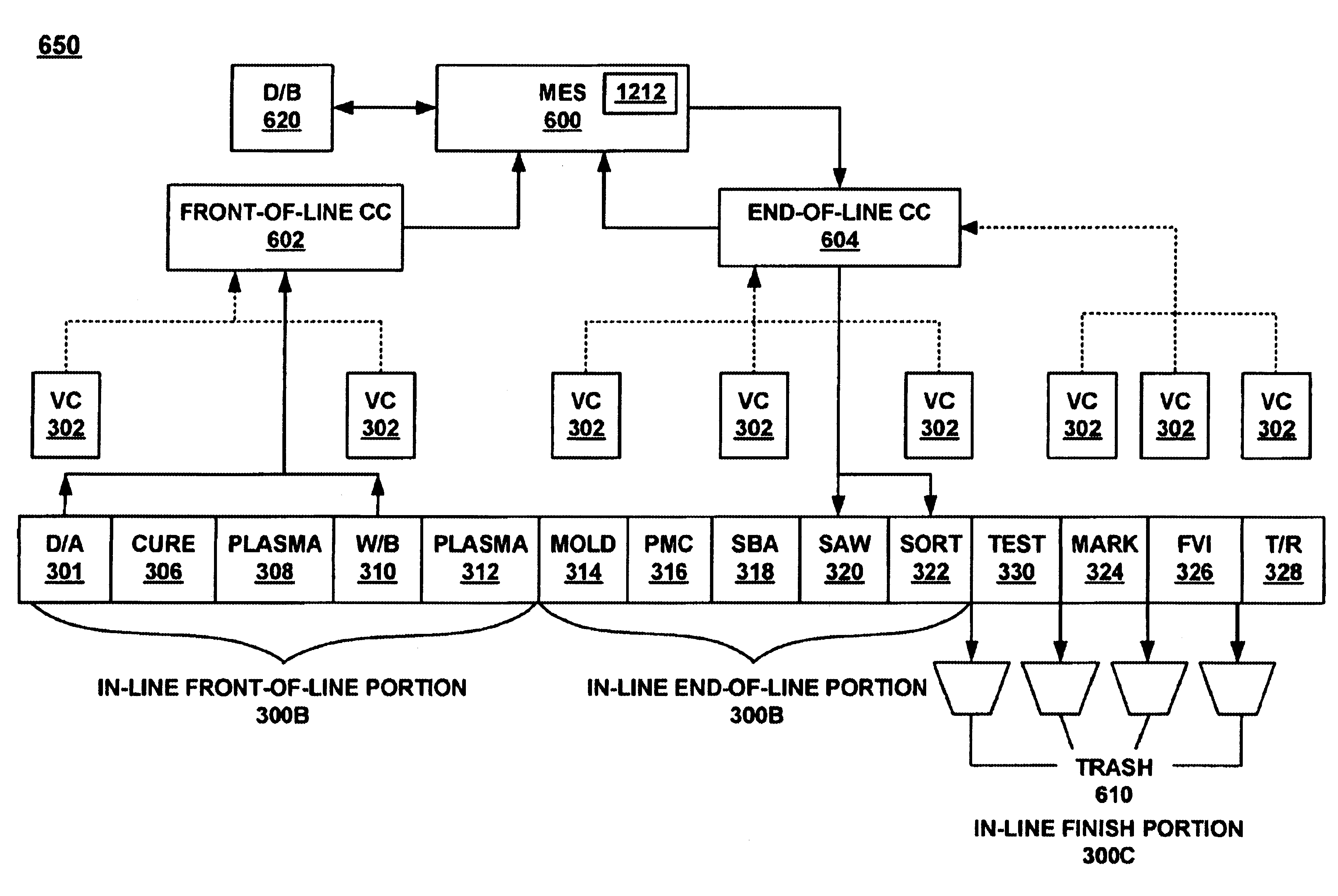
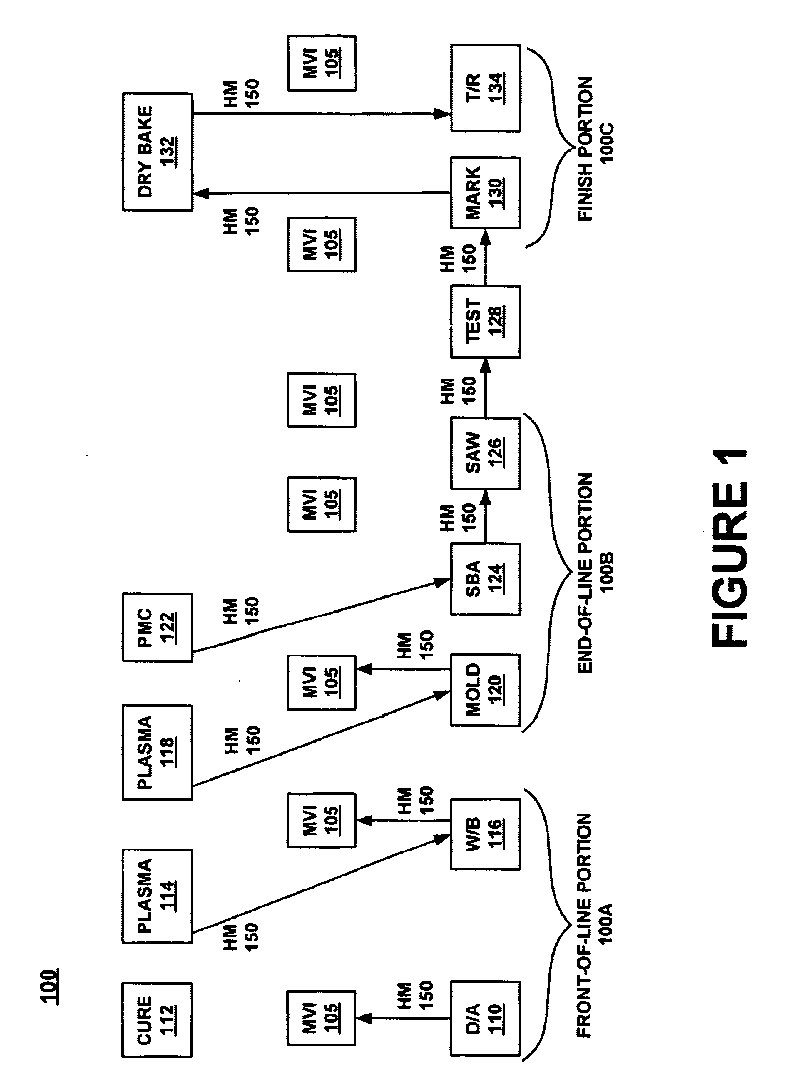
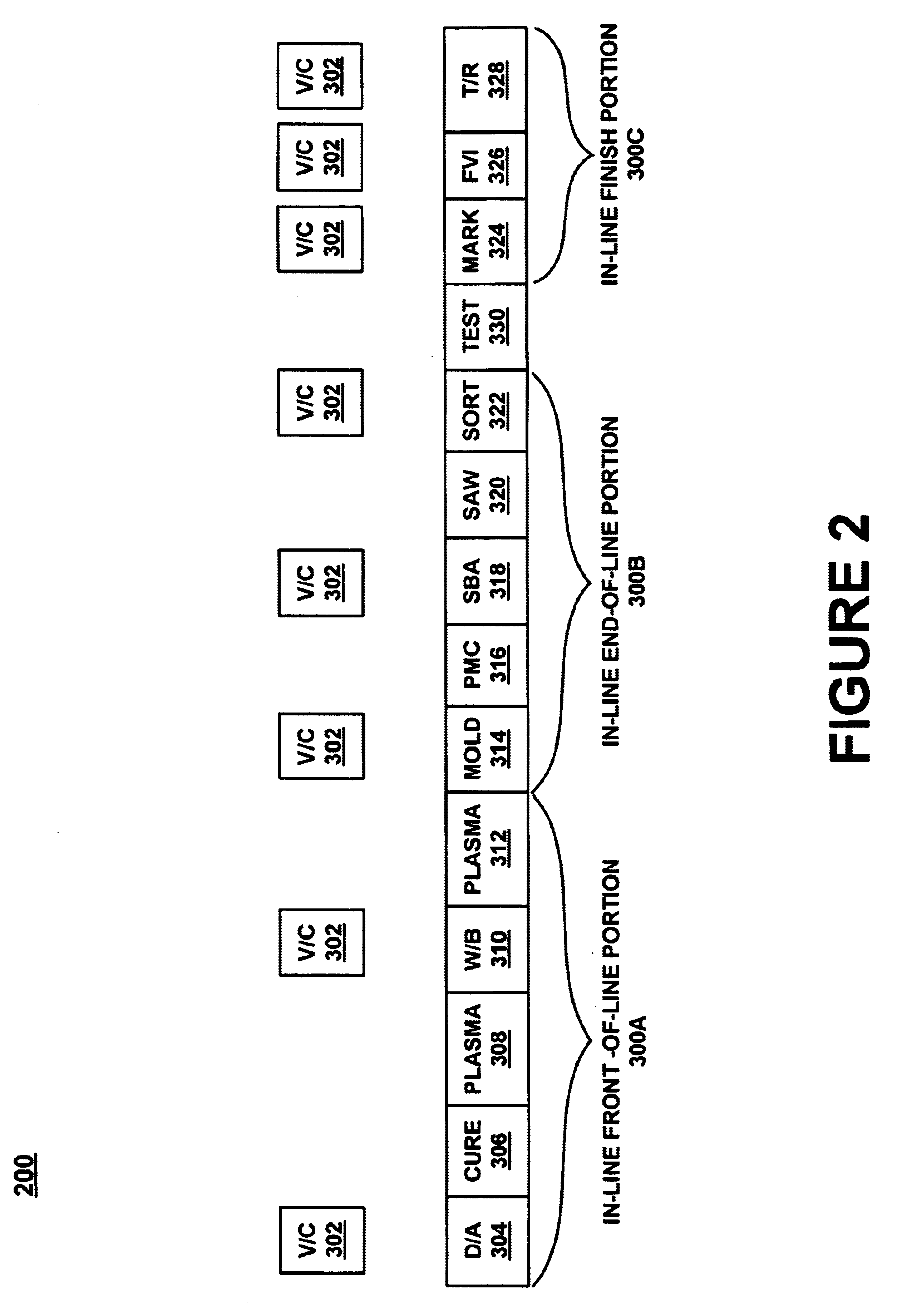
[0042]Reference will now be made in detail to the preferred embodiments of the invention, examples of which are illustrated in the accompanying drawings. While the invention will be described in conjunction with the preferred embodiments, it will be understood that they are not intended to limit the invention to these embodiments. On the contrary, the invention is intended to cover alternatives, modifications and equivalents, which may be included within the spirit and scope of the invention as defined by the appended claims. Furthermore, in the following detailed description of the present invention, numerous specific details are set forth in order to provide a thorough understanding of the present invention. However, it will be obvious to one of ordinary skill in the art that the present invention may be practiced without these specific details. In other instances, well-known methods, procedures, components, and circuits have not been described in detail as not to unnecessarily ob...


PUM

PropertyMeasurementUnit
temperatureaaaaaaaaaa
sizeaaaaaaaaaa
lengthaaaaaaaaaa

Abstract

A method and system for controlling the processing of an IC chip assembly line using a central computer system and a common communication protocol. In one embodiment, a manufacturing execution system (MEM) is used as the computer system and the communications protocol is the standard semi equipment communications standard/generic equipment model (SECS/GEM). One or more equipment cell controllers (CC) may be used to communicate between the MES a plurality of in-line substations which comprise the assembly line. Automated vision camera systems may also communicate information to the MES via the CCs. In one embodiment, the MES maintains a database in memory comprising processing history of a die-strip and results of automated die-strip examination from the vision camera systems. In one embodiment, the die-strip may be of a ball grid array (BGA) type.

Description

RELATED UNITED STATES APPLICATION[0001]This application claims priority to the provisional U.S. Patent Application Ser. No. 60 / 272,283, entitled “Automated and / or Integrated Process and / or Equipment for Assembling, Packaging, Finishing, and / or Testing,” filed Feb. 27, 2001, and assigned to the assignee of the present application which is hereby incorporated by reference.FIELD OF THE INVENTION[0002]The present invention relates to the field of IC chip manufacturing. More particularly, embodiments of the present invention relate to a method of back-end manufacturing IC packaged chips using an integrated automated back-end IC manufacturing assembly.BACKGROUND ART[0003]Conventional back-end IC manufacturing facilities, at contract assembly houses as well as several original equipment manufacturers (OEMs), have a moderate to low level of automation and equipment integration. These lines typically require several manual steps and depend upon operator intervention for many, if not nearly a...

Claims


Application Information

Patent Timeline
Patent Type & Authority Patents(United States)
IPC IPC(8): G05G15/00H01L21/00H01L21/66
CPCH01L21/67276H01L22/20H01L2924/014H01L2924/0002H01L2924/00
Inventor CHANG, BO SOON
Owner MONTEREY RES LLC
Why Eureka
Try Eureka