Microlithography reduction objective and projection exposure apparatus

a technology of projection exposure and microlithography, which is applied in the direction of mountings, optics, instruments, etc., can solve the problems of inability to achieve the incidence angle and the short distance between the wafer and the mirror arranged next to the wafer, and the instability of thin mirrors, etc., to achieve the effect of efficient masking of undesired light, easy manufacturing and mechanical achievemen

Inactive Publication Date: 2005-06-07
CARL ZEISS STIFTUNG
View PDF7 Cites 39 Cited by
  • Summary
  • Abstract
  • Description
  • Claims
  • Application Information

AI Technical Summary

Benefits of technology

[0018]An aperture stop which physically lies between the second mirror, S2, and the first mirror, S1, must be formed at least partially as a narrow ring in order to avoid clipping of light moving from S1 to S2. In such a design, there is a danger that undesirable direct light or light reflected on S1 and S2, will pass outside the aperture ring and reach the image plane and thus the wafer. However, if the aperture stop is placed in the light path between the second and third mirror and physically close to the first mirror (which can be easily achieved mechanically), an efficient masking of this undesired light is possible. The aperture stop can be designed both as an opening in the first mirror or an opening which is arranged behind the first mirror.
[0019]In another embodiment of the invention, the aperture stop is arranged on or near the second mirror. Arrangement of the aperture on a mirror has the advantage that it is easier to manufacture.

Problems solved by technology

Such asphericities and angles of incidence are not practicable in the EUV region due to the high requirements for surface quality and reflectivity of the mirrors.
Another disadvantage of the objectives disclosed in U.S. Pat. No. 5,686,728, which precludes their use with wavelengths below 100 nm such as the 11 nm and 13 nm wavelengths desirable for EUV microlithography, is the short distance between the wafer and the mirror arranged next to the wafer.
Due to the extreme layer stress in the multilayer systems discussed for 11 nm or 13 nm wavelengths, such thin mirrors are very unstable.
This projection objective also has the disadvantage that at least two of the six mirrors have very high asphericities of 26 and 18.5 μm.
However, even in the EP 779,528 arrangement, the optical free working distance between the mirror next to the wafer and the wafer itself is so small that either instabilities occur or the mechanical free working distance is negative.

Method used


Image

  • Microlithography reduction objective and projection exposure apparatus
  • Microlithography reduction objective and projection exposure apparatus
  • Microlithography reduction objective and projection exposure apparatus

Examples


Embodiment Construction

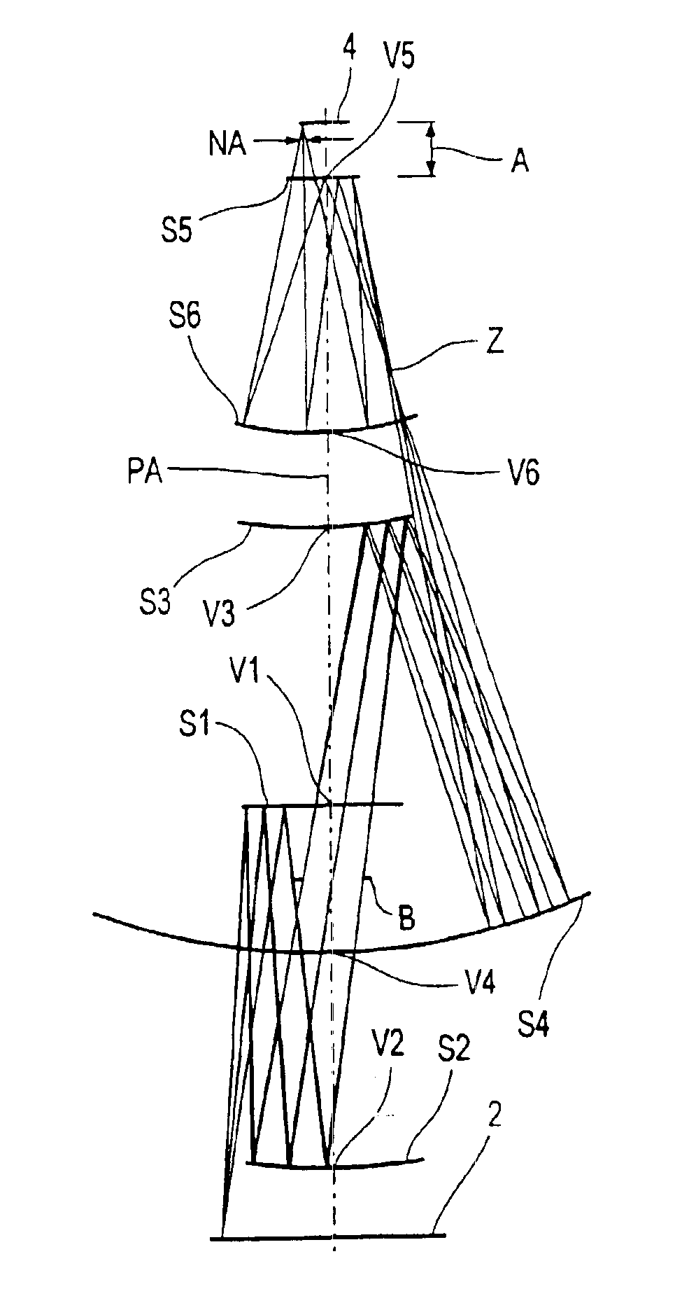
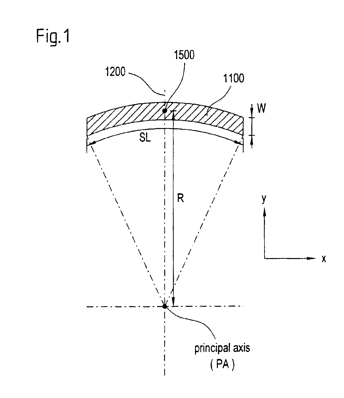
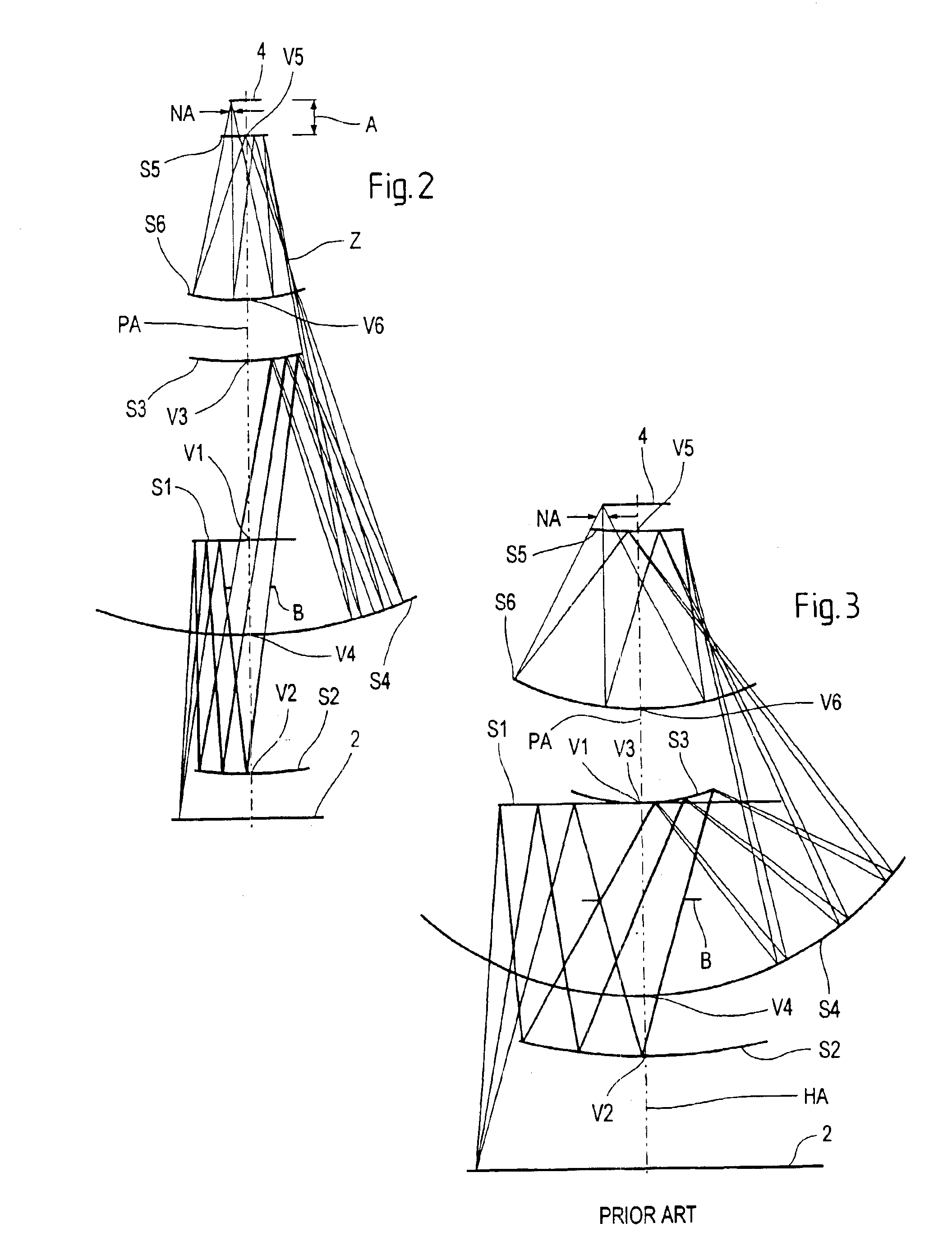
[0038]In FIG. 1 the object field 1100 of a projection exposure apparatus in the object plane of the projection objective according to the invention is shown. The object plane is imaged by means of the projection objective in an image plane, in which a light sensitive object, for example a wafer with a light sensitive material is arranged. The image field in the image plane has the same shape as the object field. The object (or the image) field 1100 has the configuration of a segment of a ring field, and the ring field has an axis of symmetry 1200.

[0039]In addition the axis 1200 extending to the object plane, the x-axis and the y-axis are depicted. As can be seen from FIG. 1, the axis of symmetry 1200 of the ring field runs in the direction of the y-axis. At the same time the y-axis coincides with the scanning direction of an projection exposure apparatus, which is designed as a ring field scanner. The x-direction is thus the direction that stands perpendicular to the scanning direct...


PUM

PropertyMeasurementUnit
lengthaaaaaaaaaa
lengthaaaaaaaaaa
wavelengthsaaaaaaaaaa

Abstract

A projection objective formed from six mirrors arranged in a light path between an object plane and an image plane is provided. The projection objective, in some examples, is characterized by having a physical distance between the vertexes of adjacent mirrors that is large enough to allow for the six mirrors to have sufficient thickness and stability properties to prevent surface deformations due to high layer tensions. In some embodiments, mirror thickness are such that surface deformations are prevented with mirrors having layer tensions lower than 350 MPa. Mirror surfaces may comprise multilayer systems of Mo/Be or Mo/Si layer pairs. In some examples, the physical distance between a vertex of the third mirror and a vertex of the sixth mirror (S3S6) satisfies the following relationship: 0.3×(a used diameter of the third mirror S3+a used diameter of the sixth mirror S6)<S3S6. In some examples, a ratio of a physical distance between a vertex of the first mirror and a vertex of the third mirror (S1S3) to a physical distance between the vertex of the first mirror and a vertex of the second mirror (S1S2) is within the range of: 0.5<S1S3/S1S2<2. In some examples, the physical mirror surfaces of the mirrors have a rotational symmetry with respect to a principal axis (PA). In some examples, all physical mirror surfaces are aspherical. In some examples, at most five physical mirror surfaces are aspherical. Other examples are provided, along with microlithography projection exposure apparatuses and processes for producing a microelectronic device.

Description

[0001]This application is a Continuation of U.S. application Ser. No. 10 / 004,674, filed on Dec. 3, 2001, now U.S. Pat. No. 6,600,552 issued on Jul. 29, 2003, which is a Continuation-in-Part of U.S. application Ser. No. 09 / 503,640, filed Feb. 14, 2000, now U.S. Pat. No. 6,353,470 issued on Mar. 5, 2002.FIELD OF THE INVENTION[0002]The invention relates to a microlithography objective, a projection exposure apparatus containing the objective, and a method of manufacturing an integrated circuit using the same.BACKGROUND OF THE INVENTION[0003]Using a lithography system operating with wavelengths below 193 nm for imaging structures of below 130 nm resolution has been proposed. In fact, such lithography systems have been suggested for the extreme ultraviolet (EUV) range with wavelengths of λ=11 nm or λ=13 nm producing structures of below 100 nm. The resolution of a lithographic system is described by the following equation:RES=k1·λ / NAwhere k1 is a specific parameter of the lithographic pro...

Claims


Application Information

Patent Timeline
Patent Type & Authority Patents(United States)
IPC IPC(8): G02B17/06G02B17/00G03F7/20
CPCG02B17/0657G03F7/70275G03F7/70233
Inventor DINGER, UDO
Owner CARL ZEISS STIFTUNG
Why Eureka
Try Eureka