Electron optical system, charged-particle beam exposure apparatus using the same, and device manufacturing method

a technology of electron beam and exposure apparatus, applied in the field of electron optical system, can solve the problems of low productivity, difficult operation of electron beams independently, trajectories and aberrations changing, etc., and achieve the effects of high reliability, high precision and improved electron optical system

Inactive Publication Date: 2005-06-07
CANON KK
View PDF60 Cites 26 Cited by
  • Summary
  • Abstract
  • Description
  • Claims
  • Application Information

AI Technical Summary

Benefits of technology

[0008]The present invention has been made to overcome the conventional drawbacks, and has as its principal object to provide an improvement of the prior art. It is an object of the present invention to provide an electron optical system which realizes various conditions such as downsizing, high precision, and high reliability at a high level. It is another object of the present invention to provide an electron optical system improved by reducing crosstalk unique to a multi-beam. It is still another object of the present invention to provide a high-precision exposure apparatus using the electron optical system, a high-productivity device manufacturing method, a semiconductor device production factory, and the like.

Problems solved by technology

This method suffers from many problems as a mass-production exposure apparatus because of a low throughput.
This method is advantageous to a simple repetitive pattern, but disadvantageous to a random pattern such as a logic interconnection pattern in terms of the throughput, and a low productivity disables practical application.
In the prior art, if many aperture electrodes are arrayed, and different lens actions are applied to electron beams, the trajectories and aberrations change under the influence of the surrounding electrostatic lens field, and so-called crosstalk occurs in which electron beams are difficult to operate independently.

Method used


Image

  • Electron optical system, charged-particle beam exposure apparatus using the same, and device manufacturing method
  • Electron optical system, charged-particle beam exposure apparatus using the same, and device manufacturing method
  • Electron optical system, charged-particle beam exposure apparatus using the same, and device manufacturing method

Examples


Embodiment Construction

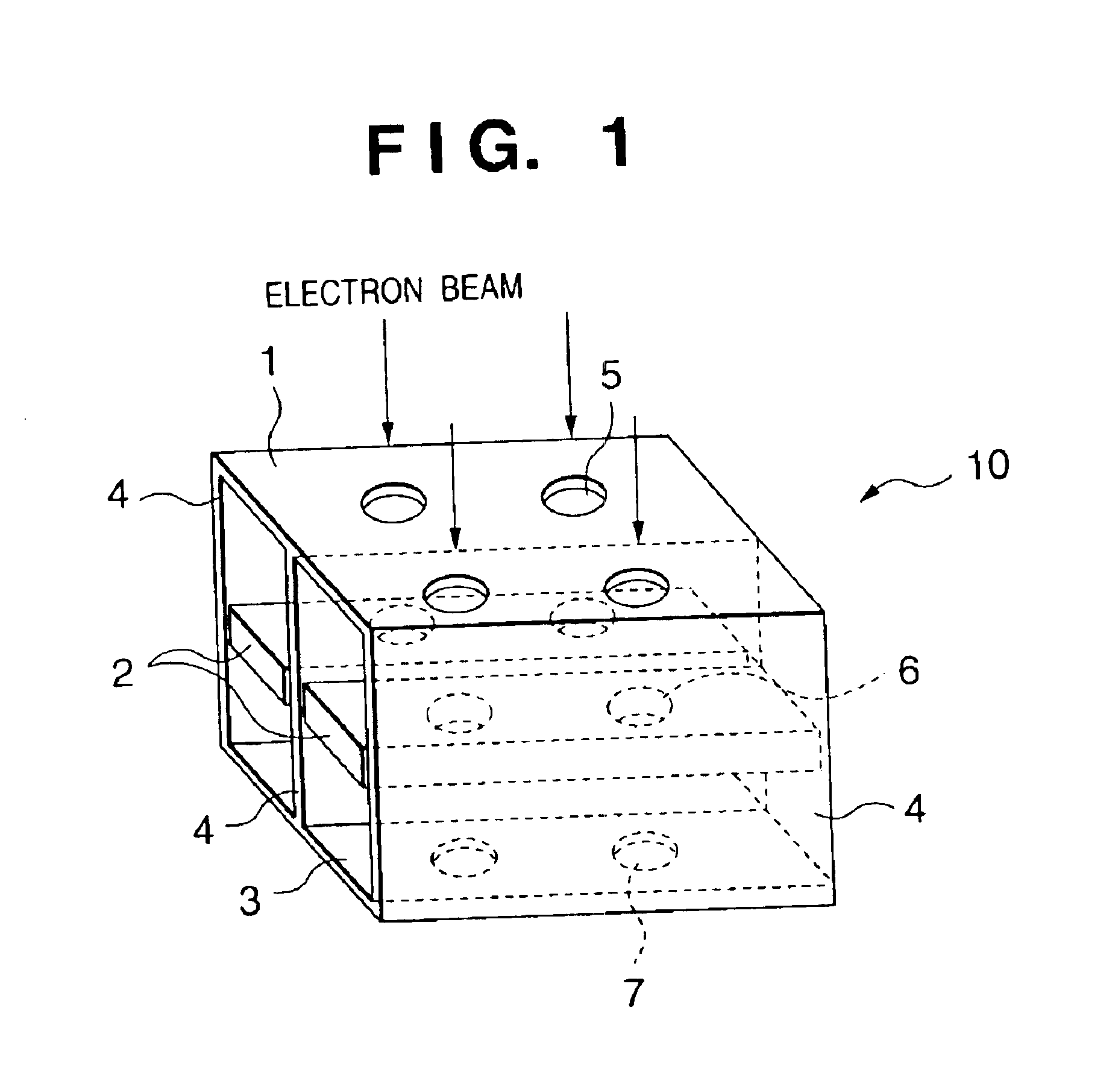
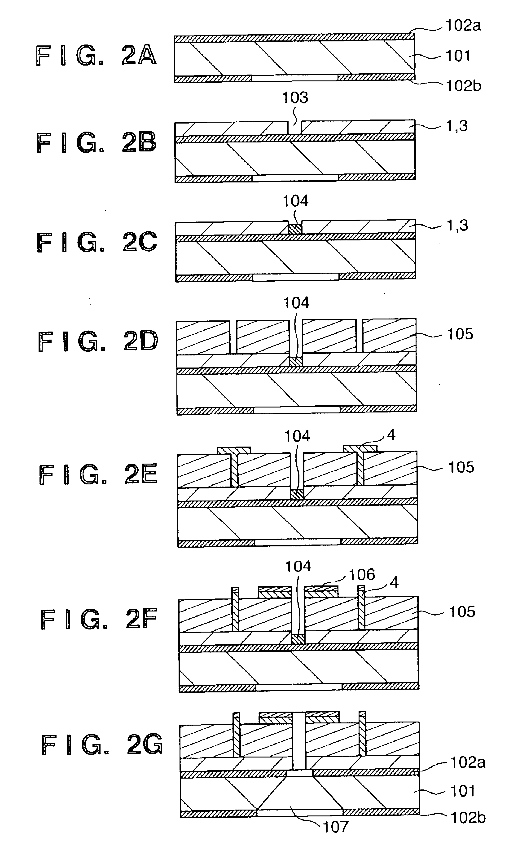
[0037]An electron optical system array according to the first embodiment of the present invention will be described. FIG. 1 is a perspective view showing an electron optical system array 10 having a plurality of electron lenses. In FIG. 1, the electron optical system array 10 is mainly constituted by sequentially stacking an upper electrode 1, a plurality of middle electrodes 2, and a lower electrode 3, each of which has a plurality of apertures. The electrodes 1, 2, and 3 form a so-called einzel lens. The middle electrodes 2 are aligned within one plane, and a conductive shield 4 for electromagnetically shielding the middle electrodes 2 is interposed between adjacent middle electrodes 2. The middle electrode 2 and shield 4 are spatially separated or connected via an insulator so as not to electrically connect them. The shield 4 is coupled to the upper and lower electrodes 1 and 3. The upper electrode 1 has a thin-film structure 10 μm in thickness that is formed from an electrode la...


PUM

PropertyMeasurementUnit
angleaaaaaaaaaa
angleaaaaaaaaaa
widthaaaaaaaaaa

Abstract

An electron optical system has a plurality of electron lenses. The system includes a first electron optical system array having electrodes with a plurality of rectangular apertures, and a second electron optical system array having electrodes with a plurality of rectangular apertures. The first and second electron optical system arrays are arranged along an optical axis in which a long side of each aperture of the first electron optical system array is perpendicular to a long side of each aperture of the second electron optical system array.

Description

FIELD OF THE INVENTION[0001]The present invention pertains to the technical field of an electron optical system suitable for an exposure apparatus using charged-particle beams such as electron beams, and relates to an electron optical system having an array of a plurality of electron lenses.BACKGROUND OF THE INVENTION[0002]In production of semiconductor devices, an electron beam exposure technique receives a great deal of attention, as a promising candidate of lithography, capable of micro-pattern exposure at a line width of 0.1 μm or less. There are several electron beam exposure methods. An example is a variable rectangular beam method of drawing a pattern with one stroke. This method suffers from many problems as a mass-production exposure apparatus because of a low throughput. To attain a high throughput, there is proposed a pattern projection method of reducing and transferring a pattern formed on a stencil mask. This method is advantageous to a simple repetitive pattern, but d...

Claims


Application Information

Patent Timeline
Patent Type & Authority Patents(United States)
IPC IPC(8): H01J37/12H01J37/10G03F7/20H01J37/04H01J37/305H01L21/027
CPCH01J37/12H01J2237/31774H01J2237/1205
Inventor ONO, HARUHITOYAGI, TAKAYUKI
Owner CANON KK
Why Eureka
Try Eureka