Optical device, and optical transceiver and other optical apparatuses using the optical device

Inactive Publication Date: 2005-06-07
ORMON CORP
View PDF15 Cites 5 Cited by
  • Summary
  • Abstract
  • Description
  • Claims
  • Application Information

AI Technical Summary

Benefits of technology

[0035]This twin core/single core conversion adapter makes it possible to connect a twin-core cord and a single-core cord to each other by connecting the second and third optical fibers to the twin-core cord and connecting the first optical fiber to the single-core cord. That is, “conversion” from a twin-core cord to a single-core cord is enabled.
[0

Problems solved by technology

However, it is difficult to register the grooves of the respective mold plates 2 with each other with high accuracy.
Further, as the diameter of the cavity 3 decreases, it becomes more difficult to pour transparent resin into the cavity 3; that is, it becomes more difficult to produce the optical device 1A with high accuracy.
However, in the optical transceiver 8 having the above structure, since the sending l

Method used


Image

  • Optical device, and optical transceiver and other optical apparatuses using the optical device
  • Optical device, and optical transceiver and other optical apparatuses using the optical device
  • Optical device, and optical transceiver and other optical apparatuses using the optical device

Examples


embodiment 1

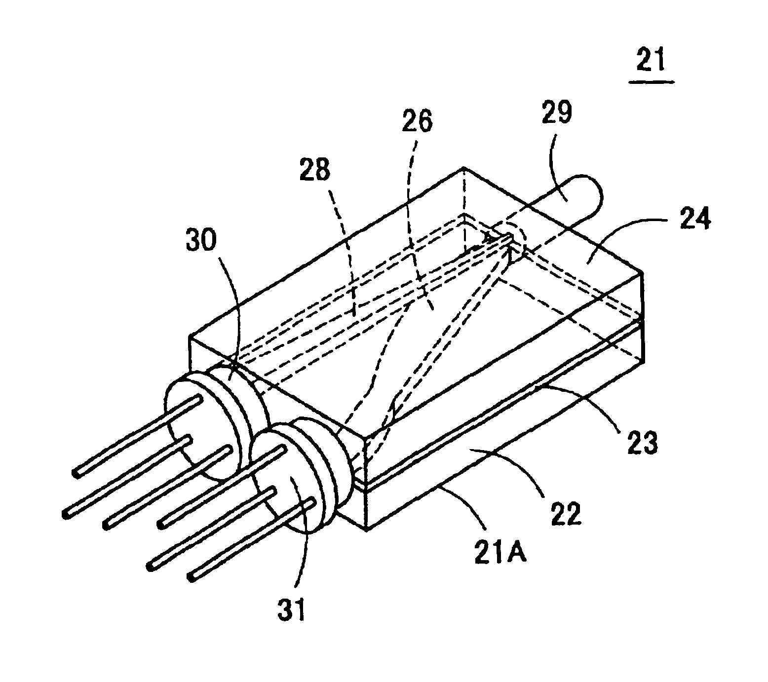
[0084]FIG. 4 is a perspective view showing how an optical transceiver 21 according to a first embodiment of the present invention is used. FIG. 5 is an exploded perspective view of an optical device 21A that is used in the optical transceiver 21. The optical device 21A is composed of a reception-side substrate 22, a cladding layer (isolation layer) 23, and a sending-side substrate 24. The reception-side substrate 22 and the sending-side substrate 24 are integrated with each other, that is, bonded to each other, with the cladding layer 23 interposed in between.

[0085]The reception-side substrate 22 is composed of a substrate 22A made of a transparent resin (e.g., PMMA (polymethyl methacrylate); refractive index: 1.49) and a receiving light guide (core) 26. The top surface of the substrate 22A is formed with a groove 25 both side surfaces of which consist of a straight portion and a curved portion. The receiving light guide 26 is formed in the groove 25 by filling the groove 25 with a ...

embodiment 2

[0096]FIG. 11 is a perspective view of an optical transceiver 52 according to a second embodiment of the invention. A plurality of light input elements 30a and 30b having different emission wavelengths are attached to the light-input / reception-side end surface of the optical device 21A at positions corresponding to the sending light guide 28. A lens 32 is inserted between the end face of the sending light guide 28 and the light input elements 30a and 30b. Therefore, one of the light input elements 30a and 30b emits light, an optical signal having the emission wavelength of the one light input element 30a or 30b is gathered by the lens 32 and input to the sending light guide 28 through its end face. Further, a plurality of light-receiving elements 31a and 31b having different sensitive wavelength ranges are attached to the receiving light guide 26 of the light-input / reception-side end surface of the optical device 21A. The light-receiving elements 31a and 31b receive respective optic...

embodiment 3

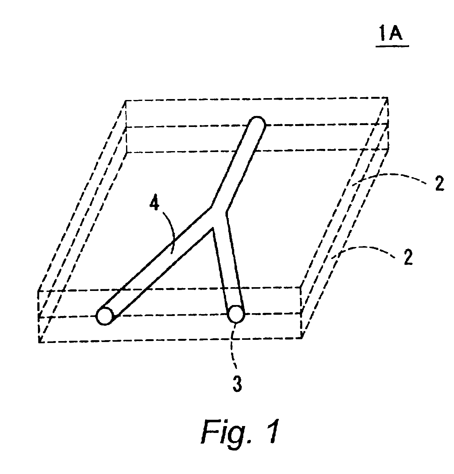
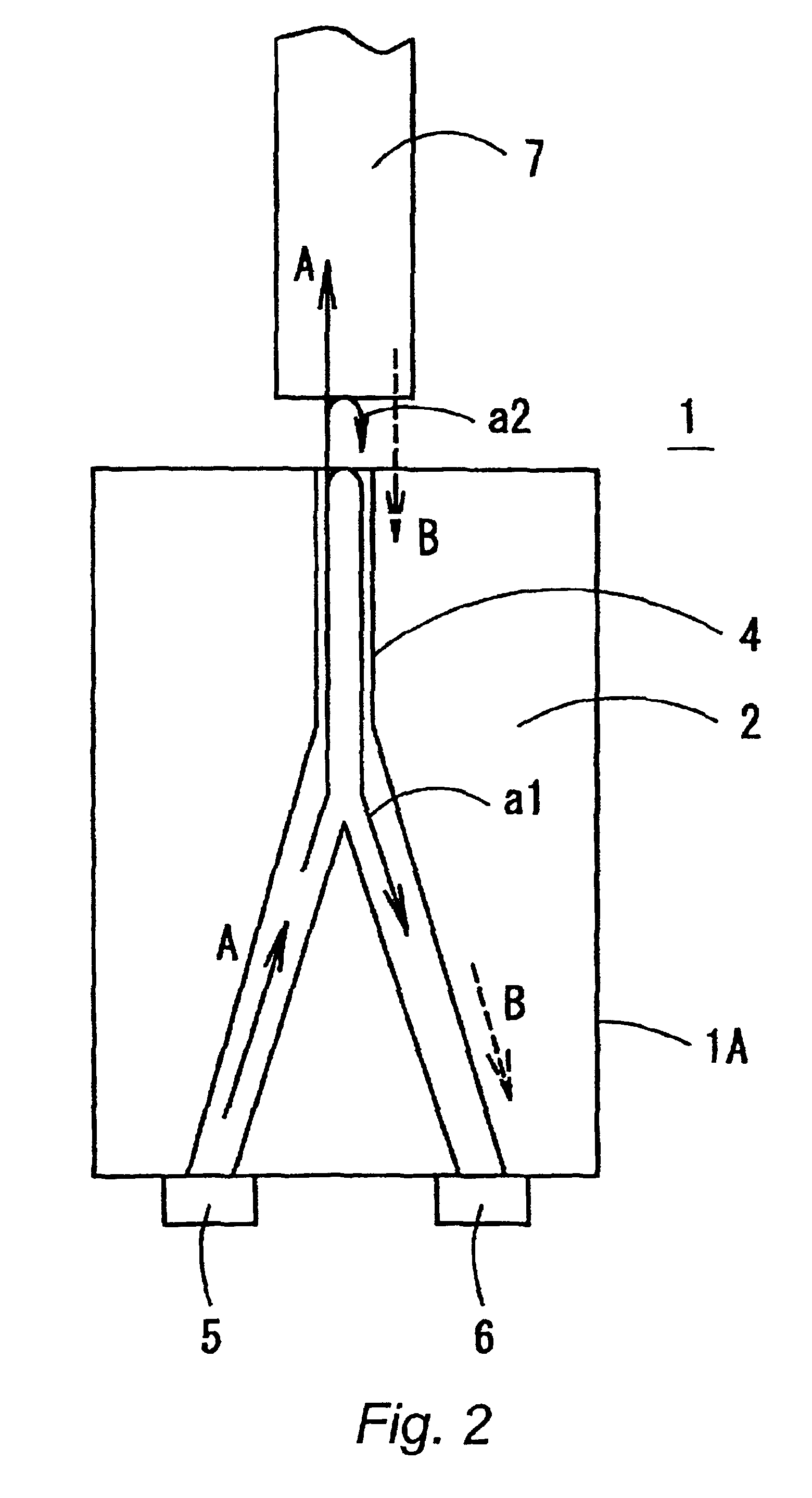
[0097]FIG. 12 is a sectional view of an optical transceiver 53 according to a third embodiment of the invention. A light-receiving element 31 is attached to the top surface, rather than the end surface, of an optical device 21A. In the optical transceiver 53, the bottom surface of the reception-side substrate 22 is formed with a triangular recess at a position corresponding to the end portion of a receiving light guide 26, whereby a total reflection surface 33 having an angle of about 45° is formed. A lens portion 34 is formed at the boundary between the receiving light guide 26 and the cladding layer 23 so as to be opposed to the total reflection surface 33. The light-receiving element 31 is fixed to the top surface of the optical device 21A. Reference numeral 35 denotes projections for positioning of the light-receiving element 31.

[0098]An optical signal coming through the receiving light guide 26 is totally reflected upward by the total reflection surface 33, gathered by the lens...


PUM


Abstract

A second light guide is formed by filling, with a core material, a groove that is formed on the top surface of a reception-side substrate. A first light guide is formed by filling, with a core material, a groove that is formed on the bottom surface of a sending-side substrate. The reception-side substrate and the sending-side substrate are bonded to each other with a cladding layer interposed in between so that the second light guide and the first light guide are isolated from each other optically.

Description

BACKGROUND OF INVENTION[0001]The present invention relates to an optical device, and an optical transceiver and other optical apparatuses using the optical device. For example, the invention relates to optical apparatuses such as an optical transceiver and a dual core / single core converter that are capable of bidirectional optical communication, that is, capable of sending and receiving an optical signal, as well as to an optical device for light wave guidance used in those apparatuses.[0002]With the recent development of high-speed, large-capacity communication networks, communication control equipment, etc., the communication using optical fibers has become the mainstream. For example, such terminals as information appliances provided in homes can send and receive a signal if they are connected to a communication network such as the Internet via optical fibers. Optical fibers are also often used in interconnecting a personal computer, a TV, a DVD player, a video game machine, etc....

Claims


Application Information

Patent Timeline
IPC IPC(8): G02B6/28G02B6/42G02B6/38G02B6/122H01L31/0232H01L33/60H01S5/022
CPCG02B6/2804G02B6/381G02B6/4246G02B6/4214G02B6/4292
Inventor YASUDA, NARUTERAKAWA, YUKARIHOSOKAWA, HAYAMI
Owner ORMON CORP
Why Eureka
Try Eureka