
Method and apparatus for self-referenced dynamic step and scan intra-field lens distortion

a dynamic step and lens distortion technology, applied in the field of optical metrology, can solve the problems of reducing the feature size of the device, affecting the alignment accuracy of the exposure tool system, and corrupting the calibration procedure of the exposure tool

Inactive Publication Date: 2005-06-14
LITEL INSTR
View PDF17 Cites 27 Cited by
  • Summary
  • Abstract
  • Description
  • Claims
  • Application Information

AI Technical Summary

Benefits of technology

[0031]Additional applications of the above outlined procedure include; improved lithographic simulation using conventional optical modeling software, advanced process control in the form of feedback loops that aut

Problems solved by technology

Increasing device densities, decreasing device feature sizes and greater overall device size conspire to make pattern overlay one of the most important performance issues during the semiconductor manufacturing process.
Intra-field overlay errors are generally related to lens aberrations or distortions, scanning irregularities, and reticle alignment.
Inaccurate overlay modeling algorithms can corrupt the exposure tool calibration procedures and degrade the alignment accuracy of the exposure tool system.
Today, these photolithographic systems are pushed to performance limits.
A problem with the this technique is two-fold, first, it is standard practice to assume that the wafer stage error is very small, randomly distributed, and can be completely accounted for using a statistical model.
In general, positional uncertainties in the wafer stage introduce both systematic and random errors, and since the intra-field is measured only in reference to the lithography tool's wafer stage, machine to machine wafer stage differences show up as inaccurate lens distortion maps.
Secondly, the assumption that lens distortion is zero at the center of the lens is incorrect.
Furthermore, the model represented by Equations 1 and 2 is entirely unsuited to modeling scanner scale overlay errors—typically the intra-field distortion model accounts only for the scanner skew and scanner scale overlay errors—in general, the synchronization errors between the reticle stage and wafer stage introduce more complex errors described below.
A drawback to this technique is that it requires that the measurements be performed on the same machine that is being assessed by this technique.
Another drawback to these techniques to determine the intra-field error is that they use the scanner itself as the metrology tool.

Method used


Image

  • Method and apparatus for self-referenced dynamic step and scan intra-field lens distortion
  • Method and apparatus for self-referenced dynamic step and scan intra-field lens distortion
  • Method and apparatus for self-referenced dynamic step and scan intra-field lens distortion

Examples


Embodiment Construction

Overview

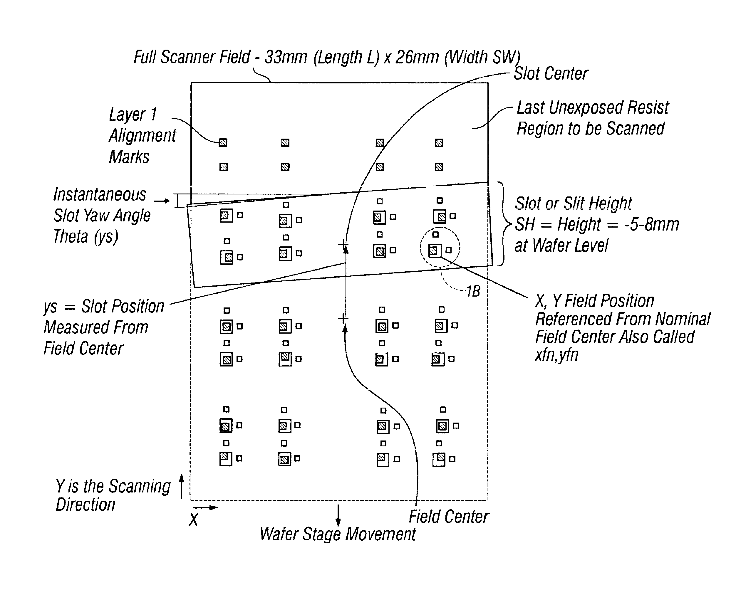
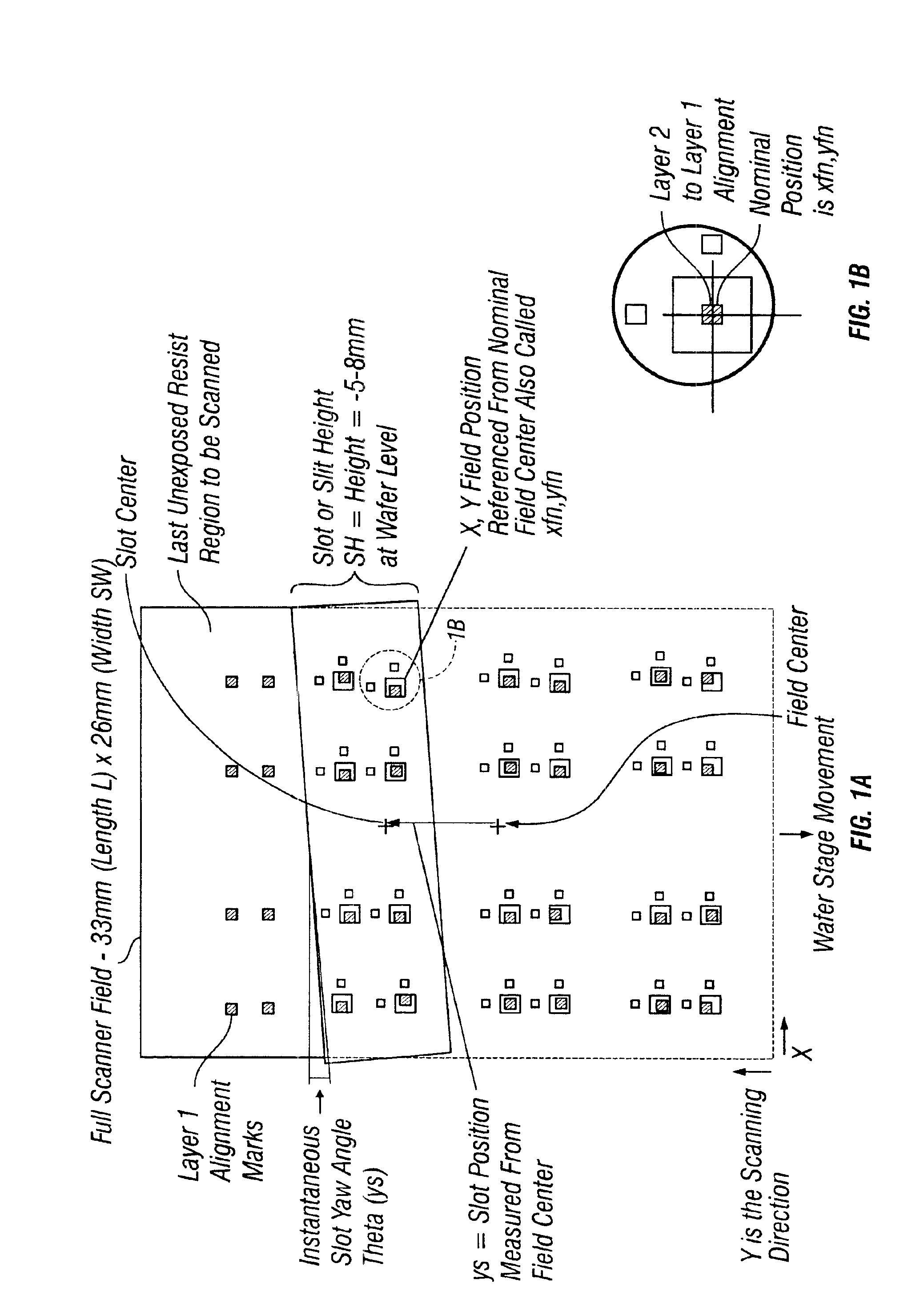
[0072]Overlay error is often referred to as registration error or pattern placement error, or simply error. Overlay error is typically classified, or divided, into the following two categories: grid or inter-field and intra-field error. Intra-field error is the overlay error in placement within a projection field, or simply field, of a lithographic projection system. Inter-field error is the overlay error from field to field on the wafer. Examples of intra-field error are illustrated in FIG. 20, and examples of inter-field errors are illustrated in FIG. 19. For photolithographic scanners the physical sources of these errors are generally distinct, with intra-field errors due to static projection lens aberrations and / or scanning dynamics while inter-field errors are due to the wafer alignment system, wafer stage and the reticle stage. An aspect described below, is determination of intra-field error produced by the lens or imaging objective optics associated with photolithogra...


PUM


Abstract

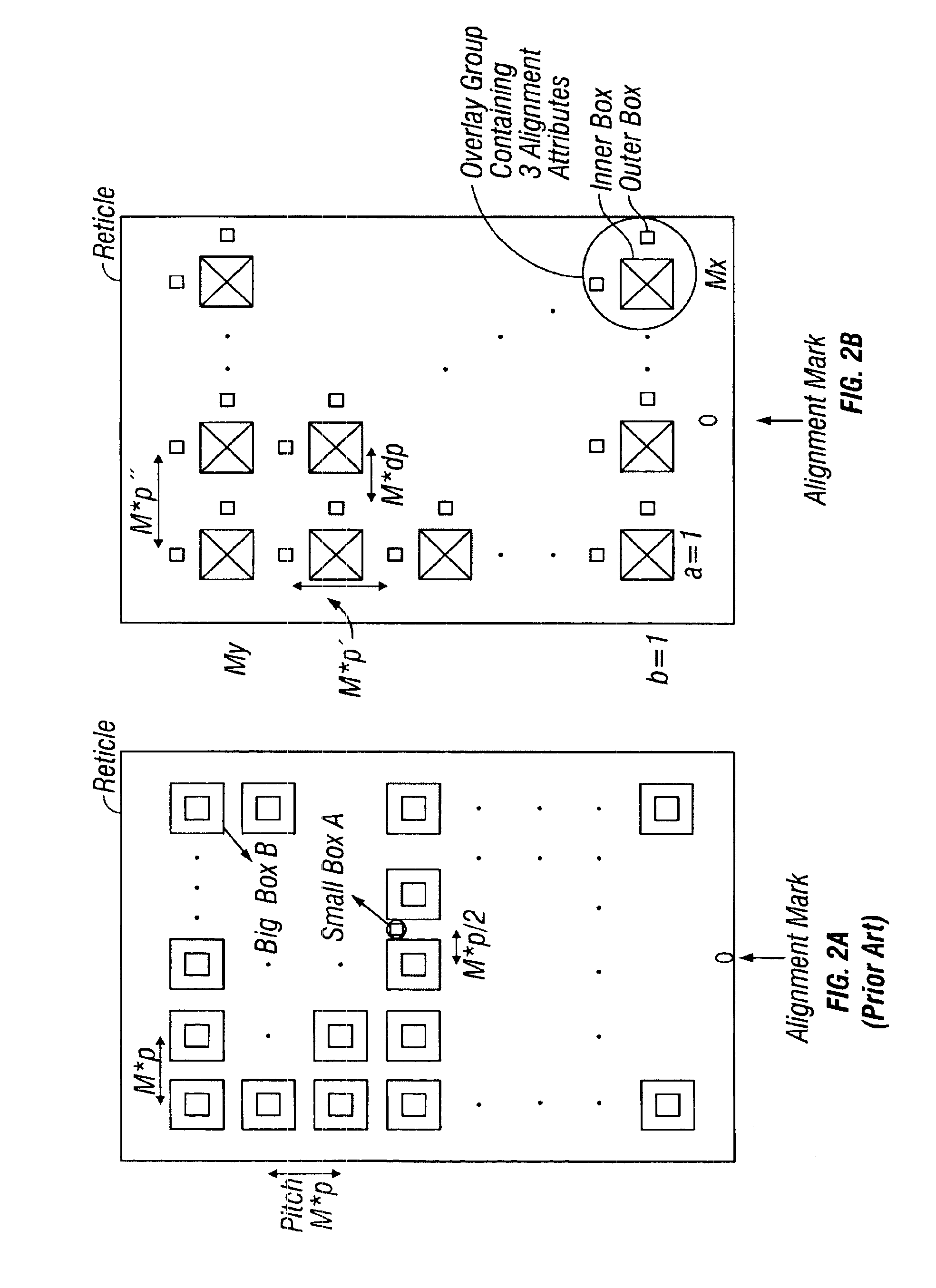
A reticle consisting of a 2-dimensional array of standard overlay targets is exposed several times onto a photoresist coated silicon wafer using a photolithographic scanner. Next, the overlay targets are measured for placement error using a conventional overlay metrology tool. The resulting overlay error data is then fed into a software program that generates the lens contribution to the intra-field error map for the photolithographic projection scanning system.

Description

REFERENCE TO PRIORITY DOCUMENT[0001]This application claims the benefit of priority of co-pending U.S. Provisional Patent Application Ser. No. 60 / 323,571, entitled “Method for Self-Referenced Dynamic Step and Scan Intra-Field Lens Distortion”, by Adlai Smith, filed Sep. 20, 2001. Priority of the filing date of Sep. 20, 2001 is hereby claimed, and the disclosure of the Provisional patent application is hereby incorporated by reference.BACKGROUND OF THE INVENTION[0002]1. Field of the Invention[0003]The present invention relates generally to optical metrology and more particularly to characterizing and monitoring intra-field distortions of projection imaging systems used in semiconductor manufacturing.[0004]2. Description of the Related Art[0005]Today's lithographic processing requires ever tighter layer-to-layer overlay tolerances to meet device performance requirements. Overlay registration is defined as the translational error that exists between features exposed layer to layer in t...

Claims


Application Information

Patent Timeline
IPC IPC(8): G03B27/42G03B27/68
CPCG03F7/70633G03B27/68
Inventor SMITH, ADLAI
Owner LITEL INSTR
Learn More