Shift register and image display apparatus using the same

a technology of shift register and image display apparatus, which is applied in the direction of logic circuit coupling/interface arrangement, pulse technique, instruments, etc., can solve the problems of increasing power consumption, increasing power consumption, and increasing power consumption of electronic circuits proportionally to frequency, so as to reduce the distance between the level shifter and the flip flop, reduce the distance for transmitting a level-shifted clock signal, and reduce the load capacity of the level shifter

Inactive Publication Date: 2005-06-21
SHARP KK
View PDF32 Cites 89 Cited by
  • Summary
  • Abstract
  • Description
  • Claims
  • Application Information

AI Technical Summary

Benefits of technology

[0014]According to the above arrangement, the shift register is provided with a plurality of the level shifters. Therefore, as compared with a construction in which a single level shifter applies a level-shifted clock signal to all flip flops, it is possible to reduce a distance between the level shifter and the flip flop. Consequently, a distance for transmitting a level-shifted clock signal can be reduced so as to cut a load capacity of the level shifter and to reduce the need for a large driving capability of the level shifter. Even when the driving capability is small and a distance is long between the ends of the flip flop, this arrangement makes it possible to eliminate the need for a buffer between the level shifter and the flip flops, thereby reducing power consumption of the shift register. Additionally, at least one of a plurality of the level shifters suspends its operation; thus, as compared with a construction in which all the level shifters are simultaneously operated, the power consumption of the shift register can be smaller. According to the above results, it is possible to achieve the shift register which can be operated by a clock signal input at a low voltage with small power consumption.

Problems solved by technology

Meanwhile, the power consumption of an electronic circuit increases proportionally to a frequency, a load capacity, and the square of a voltage.
Therefore, the longer a distance between the ends of the flip flops F1 to Fn, the longer a distance for transmission, resulting in larger power consumption.
Thus, the level shifter 103 requires a larger driving capability, thereby increasing power consumption.
Consequently, larger power consumption is necessary.

Method used


Image

  • Shift register and image display apparatus using the same
  • Shift register and image display apparatus using the same
  • Shift register and image display apparatus using the same

Examples


embodiment 1

[Embodiment 1]

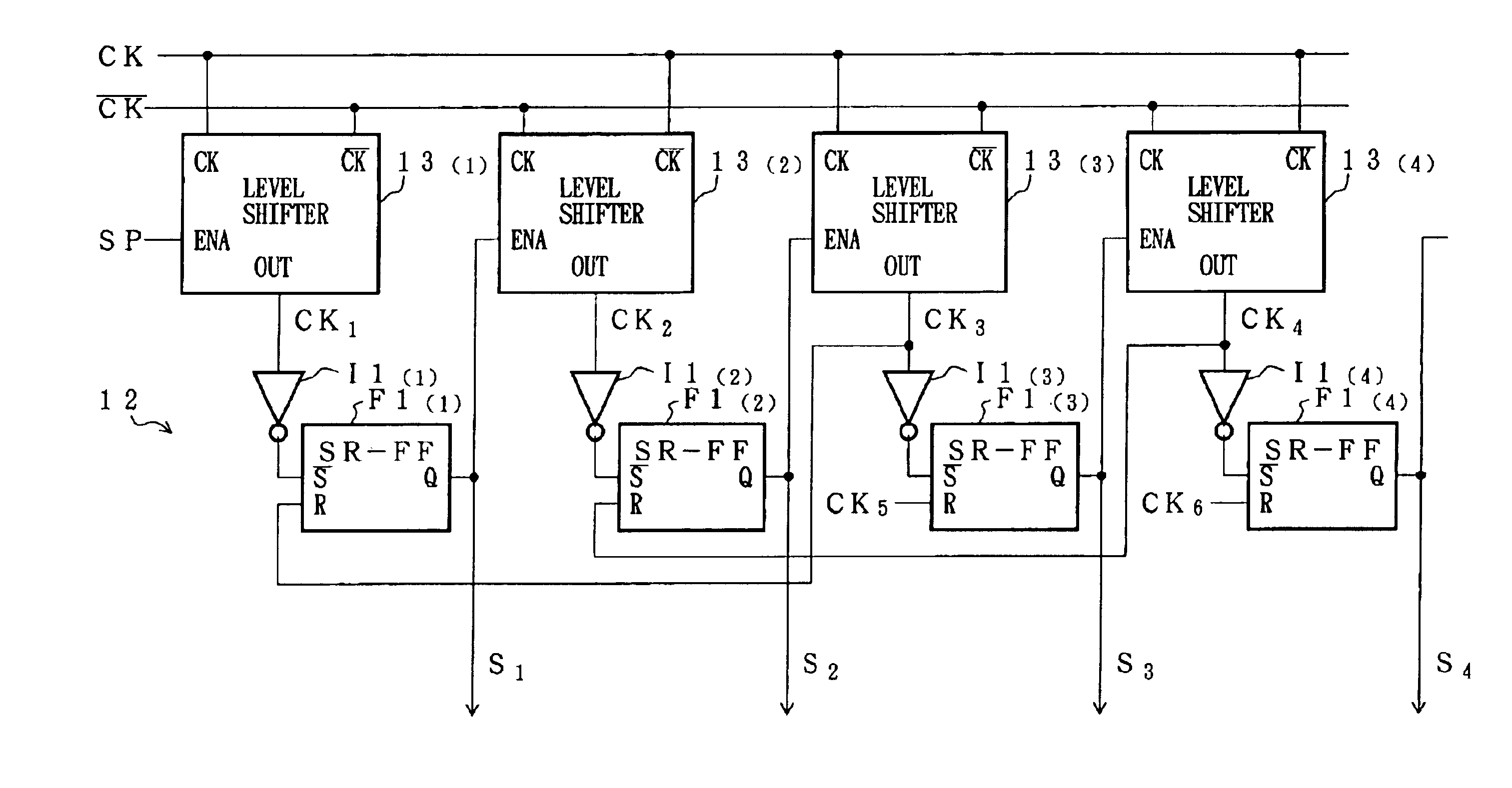
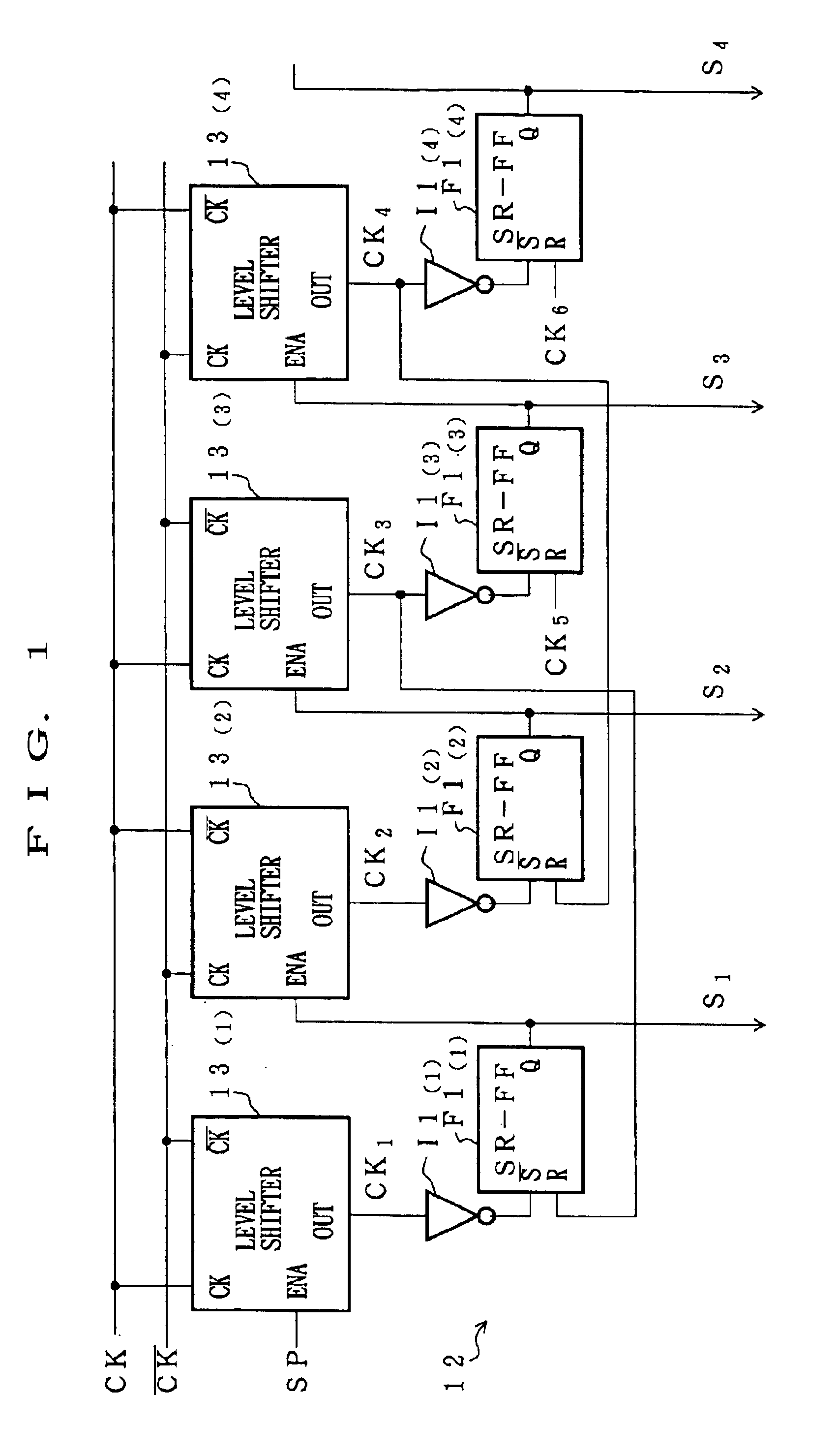
[0055]Referring to FIGS. 1 to 7, the following explanation describes one embodiment of the present invention. Here, the present invention can be widely adopted for a shift resistor, in which an inputted clock signal is smaller in an amplitude than a driving voltage. The following describes the present invention adopted for an image display apparatus as a suitable example.

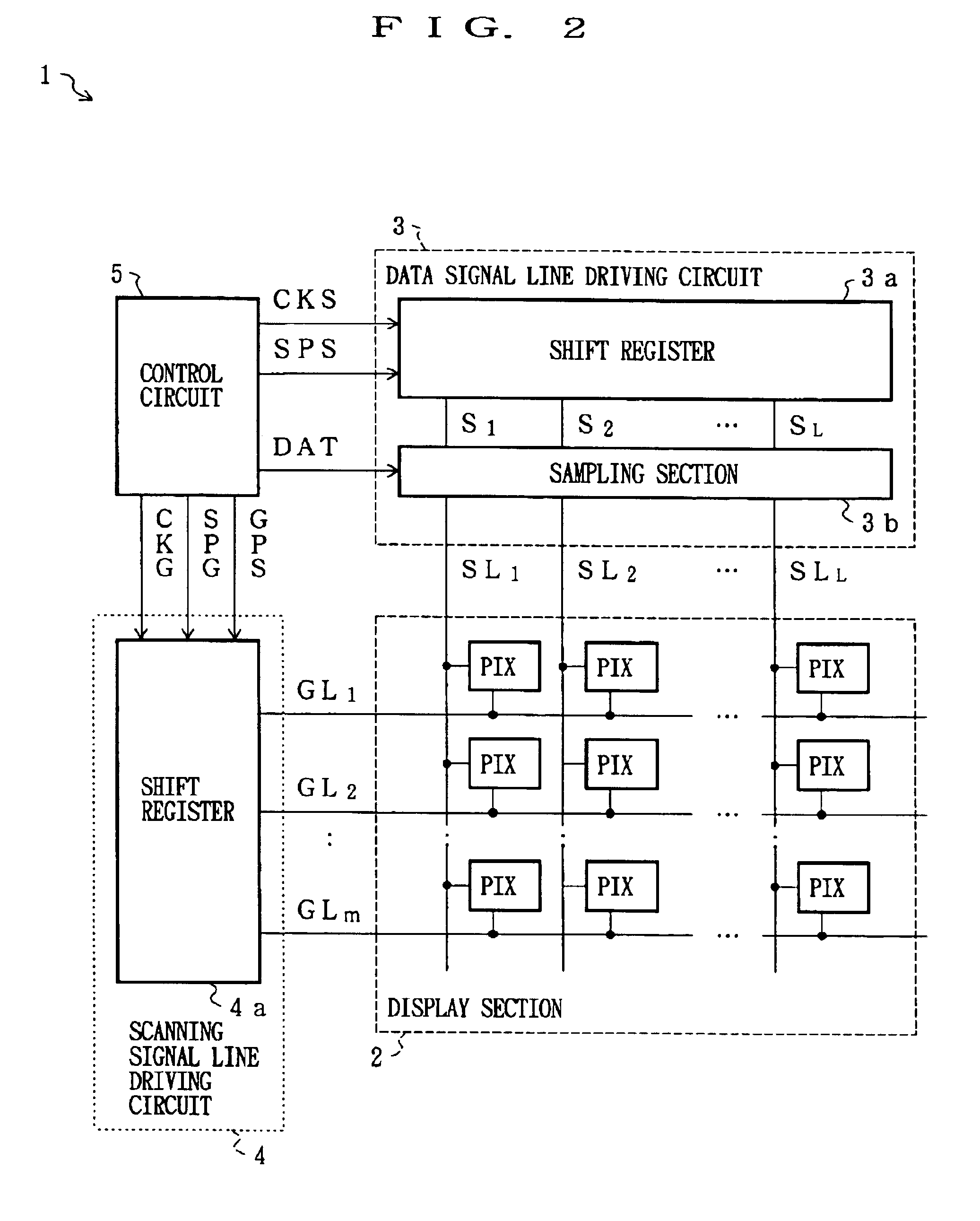
[0056]To be specific, as shown in FIG. 2, an image apparatus device 1 of the present embodiment is provided with a display section 2 having pixels PIX in a matrix form, a data signal line driving circuit 3 and a scanning signal line driving circuit 4 that drive the pixels PIX. When a control circuit 5 generates an image signal DAT for indicating a display state of the pixels PIX, the image display apparatus 1 displays an image in response to the image signal DAT.

[0057]The display section 2 and the driving circuits 3 and 4 are disposed on a single substrate to reduce the manufacturing steps and the wiri...

embodiment 2

[Embodiment 2]

[0095]Unlike Embodiment 1, referring to FIGS. 8 to 14, the following explanation discusses a construction in which a shift resistor consists of D flip flops with a plurality of steps. Here, in the following Embodiments, those members that have the same functions and that are described in Embodiment 1 are indicated by the same reference numerals and the description thereof is omitted for convenience of explanation.

[0096]Namely, as shown in FIG. 8, a shift resistor 21 of the present embodiment is provided with a flip flop section 22 consisting of a D flip flop F2(1) and later with a plurality of steps, and a level shifter 23(1) and later which are disposed respectively for the D flip flop F2(1) and later and which have the same constructions as level shifter 13(1) and later of FIG. 1.

[0097]The D flip flop F2(i) is a D flip flop in which an output Q is varied in response to an input D when a clock signal CKi is at a high level, and the output Q is maintained at a low leve...

embodiment 3

[Embodiment 3]

[0115]Incidentally, in Embodiments 1 and 2, a level shifter is provided for each flip flop. However, when a smaller circuit is considerably required, it is possible to provide a level shifter for a plurality of the flip flops, as will be described in the following Embodiments. Referring to FIGS. 15 to 19, the present embodiment describes a construction in which a level shifter is provided for a plurality of SR flip flops.

[0116]To be specific, in a shift resistor 11a of the present embodiment, as shown in FIG. 15, N pieces of SR flip flops F1 are divided for every K pieces into a plurality of blocks B1 to BP. Moreover, a level shifter 13 is disposed for each of the blocks B. Hereinafter, for convenience of explanation, a jth SR flip flop F1 in an ith block Bi is referred to as F1(i, j), where i represents an integer between 1 and P and j represents an integer between 1 and K.

[0117]Furthermore, in the present embodiment, in each block Bi, an OR circuit G2(i) is provided ...


PUM


Abstract

A level shifter 13 is provided for each of SR flip flops F1 constituting a shift register 11. The level shifter 13 increases a voltage of a clock signal CK. This arrangement reduces a distance for transmitting a clock signal whose voltage has been increased, as compared with a construction in which a voltage of a clock signal is increased by a single level shifter and the signal is transmitted to each of the flip flops; consequently, a load capacity of the level shifter can be smaller. Furthermore, each of the level shifters is operated during a pulse output of the previous level shifter 13, and the operation is suspended at the end of the pulse output. Thus, the level shifters 13 can operate only when it is necessary to apply a clock signal CK to the corresponding SR flip flop F1. As a result, even when an amplitude of a clock signal is small, it is possible to reduce power consumption of the shift resister under normal operation.

Description

FIELD OF THE INVENTION[0001]The present invention relates to a shift register which can be favorably used for, for example, a driving circuit of an image display apparatus and can shift an input pulse even when a clock signal is smaller in an amplitude than a driving voltage, and further concerns an image display apparatus using the same.BACKGROUND OF THE INVENTION[0002]For instance, in a data signal line driving circuit and a scanning signal line driving circuit of an image display apparatus, a shift register has been widely used to adjust timing when sampling each data signal from an image signal, and to generate a scanning signal applied to each scanning signal line.[0003]Meanwhile, the power consumption of an electronic circuit increases proportionally to a frequency, a load capacity, and the square of a voltage. Thus, a driving voltage has been set lower to reduce power consumption in a circuit connected to an image display apparatus, for example, in a circuit for generating an...

Claims


Application Information

Patent Timeline
Patent Type & Authority Patents(United States)
IPC IPC(8): G09G3/36G11C19/00G09G3/20
CPCG09G3/3688G09G2330/021G09G2310/0289G09G2300/0408G09G3/36
Inventor WASHIO, HAJIMEKUBOTA, YASUSHIMAEDA, KAZUHIROKAISE, YASUYOSHIBROWNLOW, MICHAEL JAMESCAIRNS, GRAHAM ANDREW
Owner SHARP KK
Why Eureka
Try Eureka