Method for fabricating an IC interconnect system including an in-street integrated circuit wafer via

a technology of integrated circuit and wafer via, which is applied in the field of interconnect systems, can solve the problems of occupying too much surface area of less expensive techniques such as laser or mechanical drilling, and restricting the length of signal path,

Inactive Publication Date: 2005-06-28
FORMFACTOR INC
View PDF31 Cites 179 Cited by
  • Summary
  • Abstract
  • Description
  • Claims
  • Application Information

AI Technical Summary

Benefits of technology

[0018]It is accordingly an object of the invention to provide an economical method for forming vertical signal paths around edges of an IC chip.

Problems solved by technology

However, since pads 20 and 26 reside in different IC packages there is a limit to how short we can make the signal path.
The lithographically-defined etching techniques described above can make small diameter, high aspect-ratio holes but these techniques are slow and expensive.
Less expensive techniques such as laser or mechanical drilling produce large holes that take up too much surface area in the IC.

Method used


Image

  • Method for fabricating an IC interconnect system including an in-street integrated circuit wafer via
  • Method for fabricating an IC interconnect system including an in-street integrated circuit wafer via
  • Method for fabricating an IC interconnect system including an in-street integrated circuit wafer via

Examples


Embodiment Construction

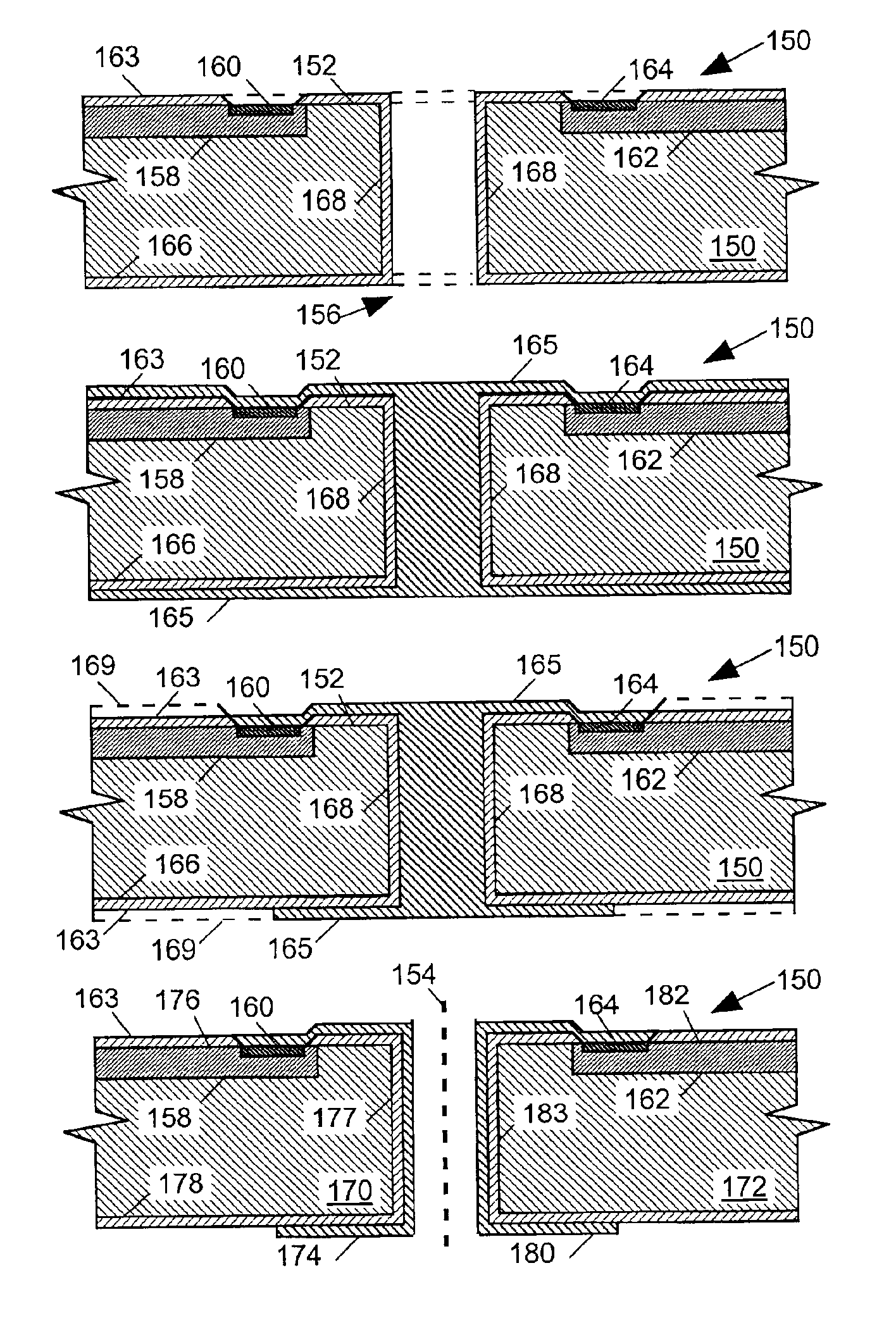
[0032]The present invention provides vertical signal paths between upper and lower surfaces of an integrated circuit (IC) semiconductor chip. In conventional IC production, ICs are fabricated in bulk as identical die forming a die matrix on a semiconductor wafer or substrate. The wafer is then cut with a saw along a series of saw-lines or “streets” located between adjacent rows and columns of the die matrix to separate the die from one another. In accordance with the invention the vertical signal paths are formed in holes extending through the street areas of the wafer.

[0033]FIG. 8 is a simplified plan view of a portion of the upper surface 152 of an IC semiconductor wafer 150 showing a pair of die 158 and 162 occupying adjacent columns of a die matrix and having respective bond pads 160 and 164 on their upper surfaces. In accordance with the invention a set of holes 156 are formed along a saw-line 154 in the street 155 between ICs 158 and 162 that a cutting tool (not shown) will fo...


PUM

PropertyMeasurementUnit
aspect ratioaaaaaaaaaa
thicknessaaaaaaaaaa
areaaaaaaaaaaa

Abstract

Vertical holes are created in streets separating individual integrated circuit (IC) dies formed on a semiconductor wafer, the holes spanning saw-lines along which the wafer is to be later cut to separate the IC die from one another to form individual IC chips. The holes are then filled with conductive material. After the wafer is cut along the saw-lines, portions of the conductive material on opposing sides of the saw-lines remain on peripheral edges of the IC chip to form signal paths between the upper and lower surfaces of the IC chips.

Description

BACKGROUND OF THE INVENTION[0001]1. Field of the Invention[0002]The present invention relates in general to electrical interconnect systems for linking integrated circuit chips and in particular to an interconnect system employing a vertical signal path along an edge of an integrated circuit chip.[0003]2. Description of Related Art[0004]FIG. 1 is a simplified sectional elevation view of a prior art interconnect system for linking two integrated circuits (ICs) 12 and 14 mounted on a printed circuit board (PCB) 10. IC 12 includes an integrated circuit chip 16 contained within an IC package 18. A bond pad 20 on the surface of chip 16 acts as an input / output (I / O) terminal for signals entering and / or departing chip 16. A typical IC will include several bond pads, but for simplicity only one is shown in FIG. 1. A bond wire 22 links bond pad 20 to a package pin 24 extending outward from package 18. Pin 24 is soldered onto a microstrip trace 25 on the surface of PCB 10. Bond wire 22 and pi...

Claims


Application Information

Patent Timeline
Patent Type & Authority Patents(United States)
IPC IPC(8): H01L25/065H01L21/70H01L21/768H01L23/498H01L23/48
CPCH01L21/76898H01L25/0657H01L25/50Y10T29/49165H01L2224/16145H01L2224/16225H01L2224/48091H01L2224/48227H01L2224/48247H01L2225/0651H01L2225/06513H01L2225/06541H01L2924/01078H01L2924/01079H01L23/49805Y10T29/49155H01L2924/00014H01L24/02H01L24/05H01L24/13H01L24/16H01L2224/0231H01L2224/02335H01L2224/02371H01L2224/02377H01L2224/05001H01L2224/05026H01L2224/05548H01L2224/05568H01L2224/05573H01L2224/131H01L2924/0001H01L2224/05599H01L2224/02H01L2924/014
Inventor MILLER, CHARLES A.
Owner FORMFACTOR INC
Why Eureka
Try Eureka