Photoresist stripper using nitrogen bubbler

a stripper and nitrogen bubble technology, applied in the field of semiconductor manufacturing, can solve the problems of affecting the surface of the wafer, affecting the cleaning effect of hollow objects, and generating contaminant particles when moving components of the stirrer, and achieve the effect of effectively stripping obscured photoresist or other organic materials

Inactive Publication Date: 2005-06-28
TAIWAN SEMICON MFG CO LTD
View PDF13 Cites 13 Cited by
  • Summary
  • Abstract
  • Description
  • Claims
  • Application Information

AI Technical Summary

Benefits of technology

[0015]It is therefore a primary object of the present invention to provide a method for effectively stripping obscured photoresist or other organic materials from semiconductor wafers having dense top surface conductive patterns with prominent sidewalls.
[0016]Another object of the present invention is to provide an apparatus that manifests a scrubbing action with a directional agitation of the viscous stripper that is against the immersed wafer's surface using nitrogen bubbles moving upward and parallel to the dense top surface conductive patterns thus increasing the collision frequency between the stripper and photoresist molecules.
[0017]It is yet another object of the present invention to increase the throughput due to the efficient stripping rate promoted by increased solubility.
[0018]It is still another object of the present invention to prolong the lifetime of the stripper by reducing the stripping process time.
[0019]It is still another object of the present invention to improve the stripping uniformity within a wafer and to eliminate the boundary condition of the tank.

Problems solved by technology

While mechanical stirring or agitation techniques have been used, the moving components of a stirrer frequently generate contaminant particles that are detrimental to the wafer surfaces.
Furthermore, from a thermodynamics point of view, the activation energy of photoresist molecules dissolving into the stripper is intensified under static conditions, thus leaving residues on the wafers in view of the fact that an incomplete chemical reaction takes place in a limited processing time.
The process suffers the risk of re-depositing the dissolved impurities onto the wafer in a viscous static stripper due to the low solubility of the photoresist.
The process of stripping the photoresist from between these three dimensional circuit lines becomes increasingly challenging, particularly on the 6 and 8 inch diameter wafers.
Residues left behind are harmful contaminants to the microscopic circuits which the fabrication process creates.
The apparatus of FIG. 1, having a rotating mechanism immersed in the process chemical, conventionally used when etching wafers, is not recommended for use during photoresist stripping or for cleaning wafers because of particulate generated by the cassette rotating drive members, hence, contaminating the process chemicals and also the wafers being processed.

Method used


Image

  • Photoresist stripper using nitrogen bubbler
  • Photoresist stripper using nitrogen bubbler
  • Photoresist stripper using nitrogen bubbler

Examples


Embodiment Construction

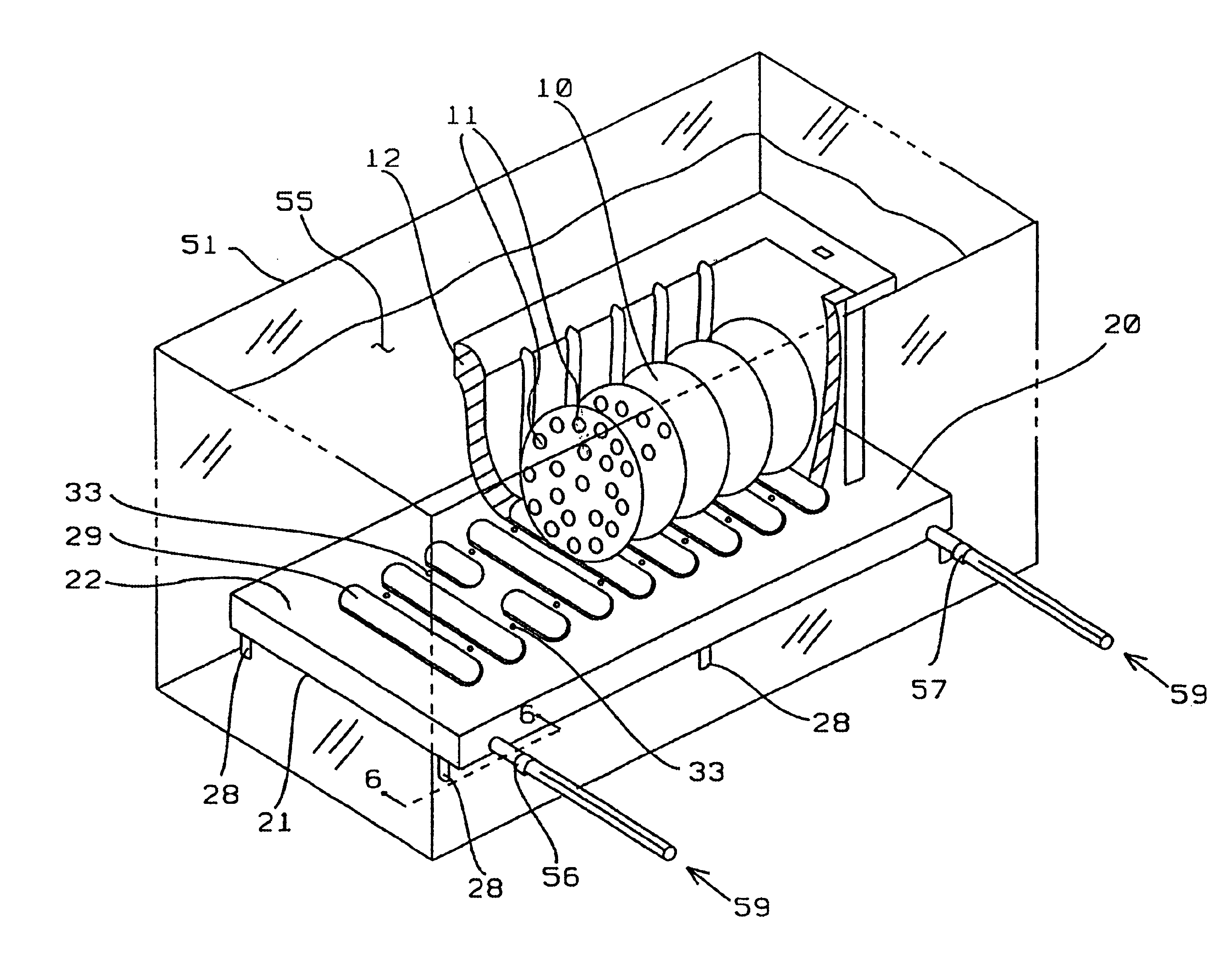
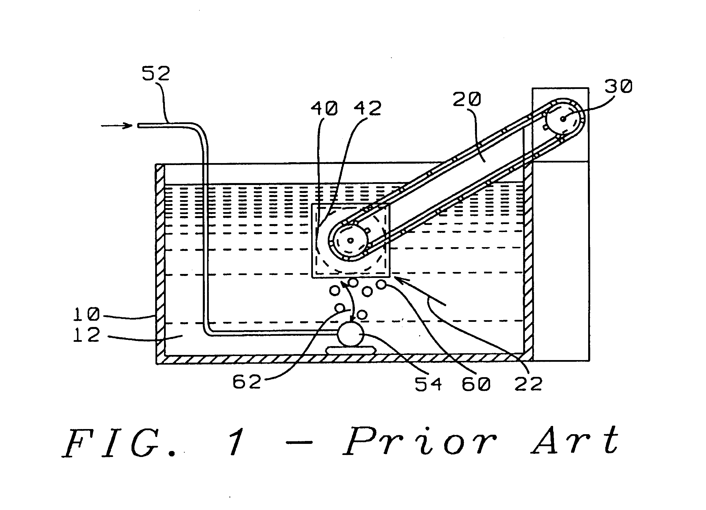
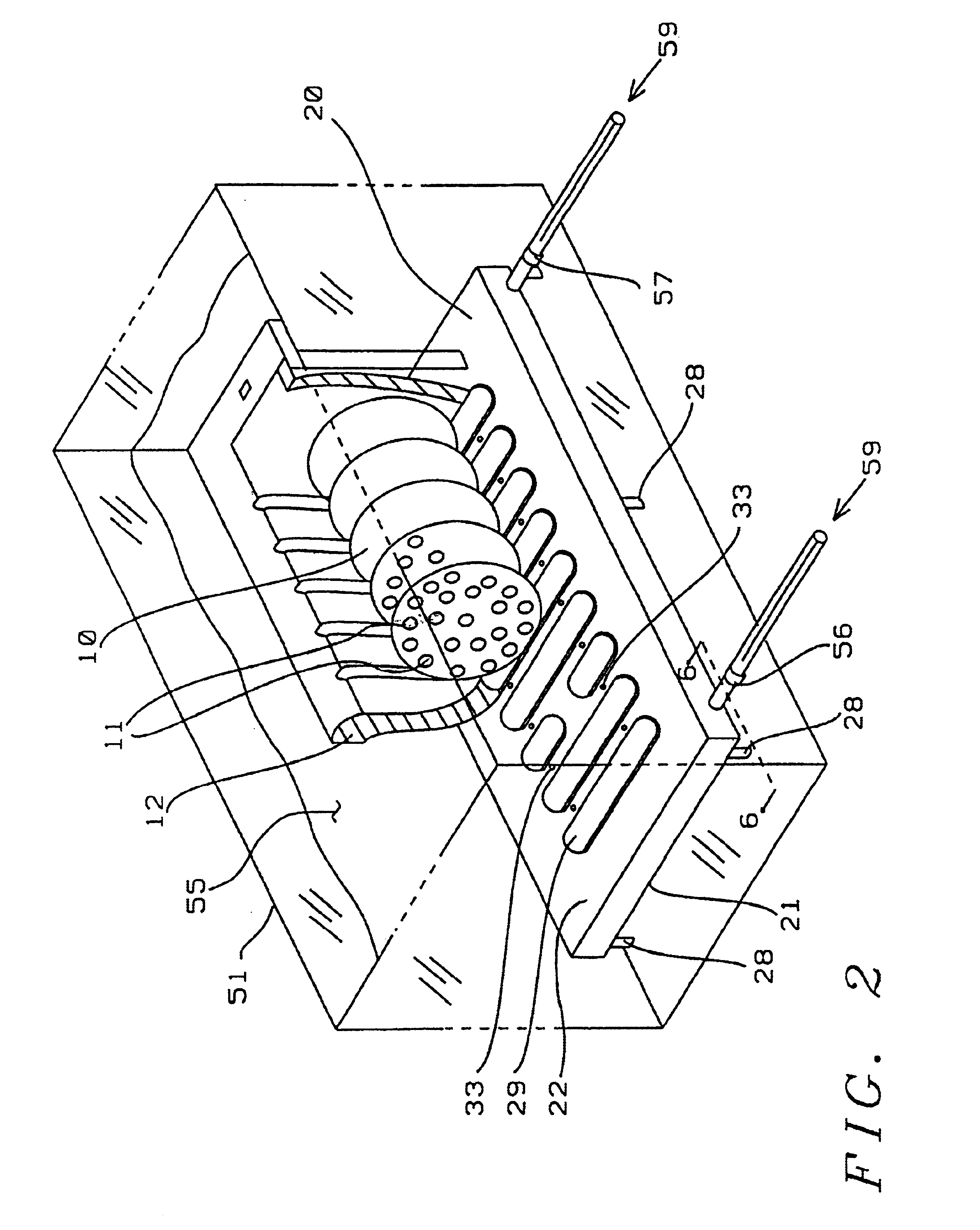
[0027]In a preferred embodiment, the process of the invention is conducted by the apparatus of FIG. 2, is characterized by a gas distribution plate 20 in which a gas supply manifold directs gas bubbles 11 from the bottom of a process tank 51 upward and between wafers 10 contained in a cassette 12 and supported therewithin. This improved method and apparatus is used for effectively stripping photoresist from the larger semiconductor wafers having dense top conductive patterns with protuberant sidewalls. The method provides a scrubbing action that is parallel to the device array being formed on the wafer's surface. Broadly stated, the method of a chemical action on large substrates supported adjacent respective edge portions thereof in a carrier includes submerging the carrier and substrates supported thereby in a process tank containing a liquid chemical, and a gas distribution plate disposed on the bottom of the tank for directing gas bubbles upward and parallel to the surfaces of e...


PUM

PropertyMeasurementUnit
diameteraaaaaaaaaa
diameteraaaaaaaaaa
flexibleaaaaaaaaaa

Abstract

Provided is a process and apparatus characterized by a gas distribution plate in which a gas supply manifold directs gas bubbles from the bottom of a process tank upward and between wafers contained in a cassette and supported therewithin. This improved method and apparatus is used for effectively stripping photoresist from the larger semiconductor wafers having dense top conductive patterns with protuberant sidewalls. The method provides a scrubbing action that is parallel to the device array being formed on the wafer's surface. Broadly stated, the method of a chemical action on large substrates supported adjacent respective edge portions thereof in a carrier includes submerging the carrier and substrates supported thereby in a process tank containing a liquid chemical, and a gas distribution plate disposed on the bottom of the tank for directing gas bubbles upward and parallel to the surfaces of each substrate contained in the carrier to ensure that a uniform chemical action occurs.

Description

BACKGROUND OF THE INVENTION[0001](1) Technical Field[0002]The present invention relates to semiconductor manufacturing. More specifically, the invention teaches an improved fluid application systems for stripping photoresist from silicon wafers, particularly wafers having dense top metal circuit patterns with sidewalls which obscure residual photoresist, and the like.[0003](2) Description of the Prior Art[0004]The following four documents relate to methods dealing with stripping and cleaning of substantially planar objects.[0005]U.S. Pat. No. 4,251,317 issued Feb. 17, 1981 to Foote, shows a gas bubbler in combination with a wafer cassette rotation within a wet wafer cleaning tank.[0006]U.S. Pat. No. 5,868,898 issued Feb. 9, 1999 to Liu et al., shows a wet wafer cleaning tank with a fluid distributor to agitate the stripper and form bubbles.[0007]U.S. Pat. No. 5,704,981 issued Jan. 6, 1998 to Kawakami et al., recites a buffer plate for distributing gas in a reactor.[0008]U.S. Pat. No...

Claims


Application Information

Patent Timeline
Patent Type & Authority Patents(United States)
IPC IPC(8): B08B5/00B08B3/10H01L21/00
CPCB08B3/102H01L21/67086Y10S438/906
Inventor CHEN, CHIE-CHITSENG, WEN-HSIANGPAN, SHENG-LIANGFANG, JEN-SHIANG
Owner TAIWAN SEMICON MFG CO LTD
Why Eureka
Try Eureka