Carbon dioxide gas laser machining method of multilayer material
a carbon dioxide and laser machining technology, applied in the direction of manufacturing tools, welding/soldering/cutting articles, printed circuit manufacturing, etc., can solve the problems of increasing the cost, difficult to fine-tune the depth direction, and stably removing the conductor layer
- Summary
- Abstract
- Description
- Claims
- Application Information
AI Technical Summary
Benefits of technology
Problems solved by technology
Method used
Image
Examples
first embodiment
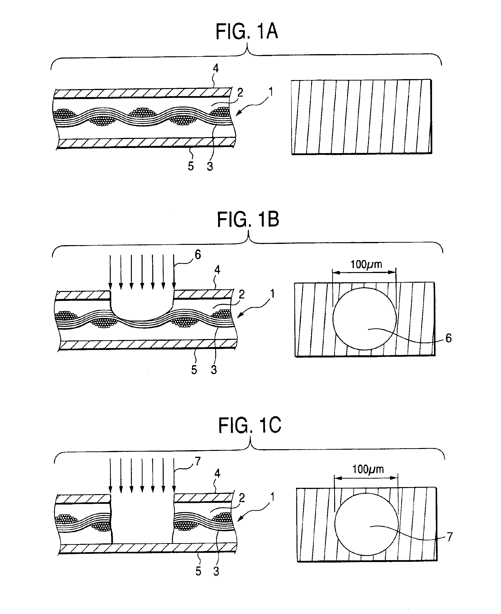
[0026]A carbon dioxide laser machining method of a multilayer material according to a first embodiment of the invention will be discussed with FIGS. 1A to 5.
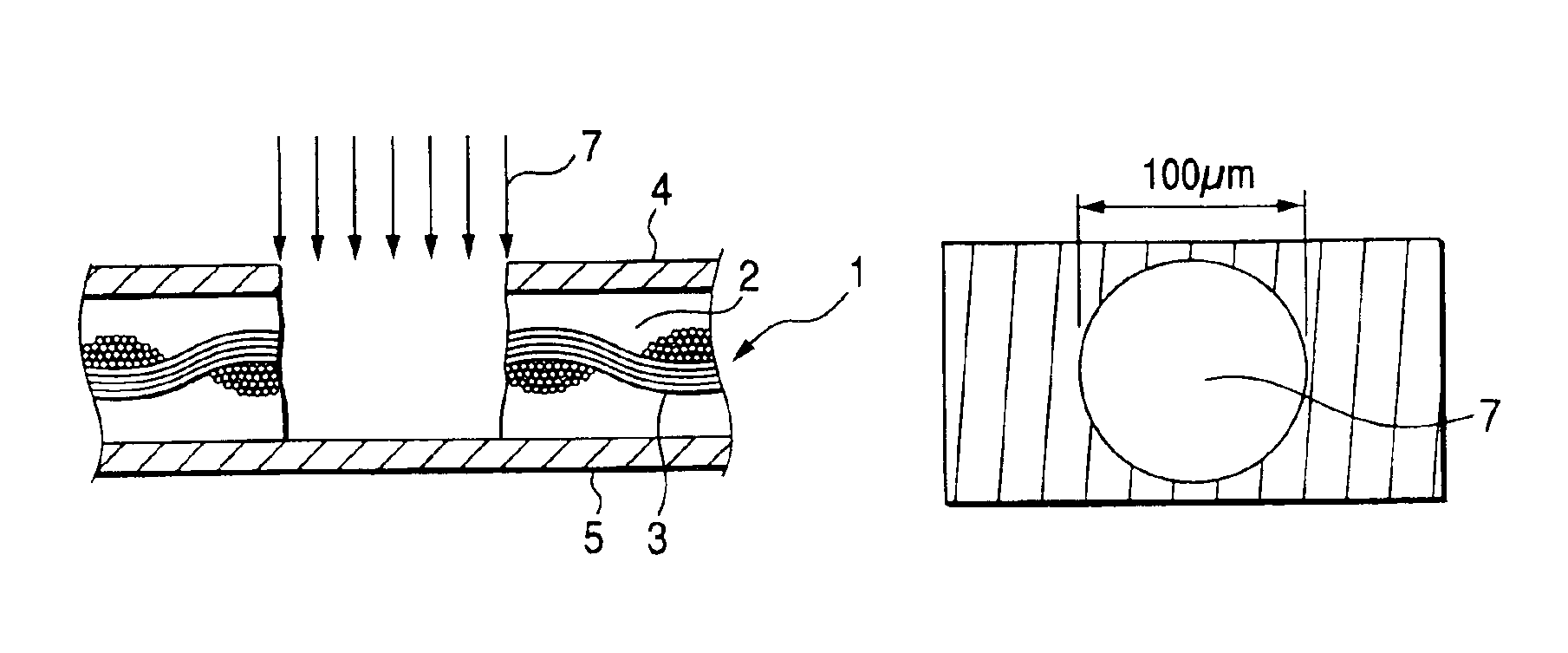
[0027]In the embodiment, a wiring board having conductor layers 4 and 5 on the surface and back of an insulation layer 1 formed by impregnating glass cloth 3 with resin 2 and hardening is formed with a blind hole to electrically connect the conductor layer 4 on the laser light incidence side and the conductor layer 5 on an opposite side.
The glass cloth 3 exists to improve the electric reliability of the board and the board strength and may be replaced with any other material and may not necessarily exist.
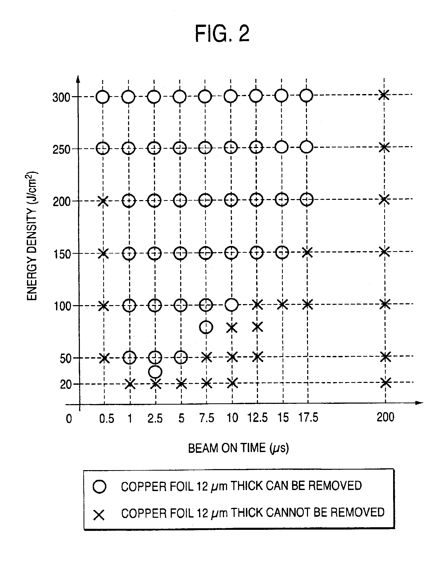
[0028]Here, the printed wiring board machined using the carbon dioxide laser machining method of a multilayer material according to the embodiment has the conductor layer 4 being copper foil 12 μm thick, the conductor layer 5 being copper foil 18 μm thick, and the board 1 being epoxy 80 μm thick as shown in FIG. 1A. The hole dia...
second embodiment
[0050]Next, a carbon dioxide laser machining method of a multilayer material according to a second embodiment of the invention will be discussed with FIGS. 6A to 8. To begin with, as shown in FIG. 6B, laser light 8 with the beam ON time being 3 μs and the energy density being 150 J / cm2 is applied to a conductor layer 4 of a wiring board as shown in FIG. 6A in area φ50 μm smaller than area φ100 μm of the conductor layer 4 to be finally removed, and the conductor layer 4 and some of an insulation layer 1 are removed. In the removal, the laser light with the beam ON time ranging from 1 μs to 10 μs and the energy density being 25 J / cm2 or more is used and thus the energy of the laser light is used to efficiently remove the conductor layer 4 and extra laser light does not machine the insulation layer 1 unnecessarily largely, so that it is made possible to prevent the conductor layer 4 from being projected into the hole or the hole shape from becoming a middle swell shape upon application...
PUM
| Property | Measurement | Unit |
|---|---|---|
| Time | aaaaa | aaaaa |
| Energy density | aaaaa | aaaaa |
Abstract
Description
Claims
Application Information


