Manufacturing method of multilayer wiring board

A manufacturing method and wiring board technology, applied in multilayer circuit manufacturing, printed circuit manufacturing, processing of insulating substrate/layer, etc., can solve the problem of unreliable resin surface, unsuitable for fine processing, reduced heat resistance and electrical insulation Performance and other issues, to achieve the effect of improving plating adhesion, low equipment requirements, and reducing production costs

Pending Publication Date: 2021-11-02
大同共聚西安科技有限公司
View PDF0 Cites 0 Cited by
  • Summary
  • Abstract
  • Description
  • Claims
  • Application Information

AI Technical Summary

Problems solved by technology

[0004] The purpose of the present invention is to exist the possibility that the resin surface is unreliable when the existing multi-layer wiring board is manufactured by the full subtractive method, and it is not suitable for fine processing; while the rubber remaining in the insulating resin layer in the full additive method reduces the heat resistance and To solve the problem of electrical insulation performance, a method of manufacturing a multilayer wiring board is provided. When an insulating layer and a conductor layer are alternately laminated to form a multilayer wiring board, an insulating resin with copper foil formed by pre-integrating copper foil and insulating resin is provided. Bonding sheets, and forming holes by carbon dioxide laser processing, solving the above problems to obtain multilayer circuit boards with high reliability

Method used


Image

  • Manufacturing method of multilayer wiring board
  • Manufacturing method of multilayer wiring board
  • Manufacturing method of multilayer wiring board

Examples


Embodiment 1

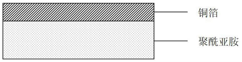
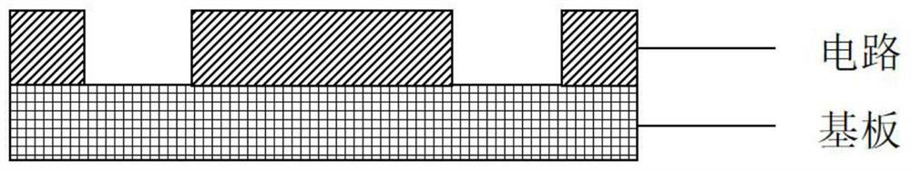
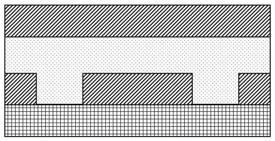
[0022] (1) Paste 20 μm copper foil on 80 μm polyimide film to obtain copper foil / polyimide two-layer film (planing diagram as attached figure 1 shown), and then place the copper foil / polyimide two-layer film on top of the circuit board (the planing diagram of the circuit board is shown in the attached figure 2 shown), put it into a hot press, raise the temperature from room temperature to 240 °C at a rate of 5 °C / min, and keep it at this temperature for 1 h under a pressure of 0.5 MPa, and then cool it to room temperature in a water cooling system, where the circuit The thickness of the circuit in the substrate is 20 μm, and the thickness of the substrate is 20 μm. The planing diagram of the obtained laminate is shown in the attached image 3 shown;

[0023] (2) use 2wt% ferric chloride aqueous solution at room temperature and 2Kgf / cm 2 The copper foil on the product obtained in step (1) is etched for 1 min under the spray pressure to form an opening on the copper foil, whe...

Embodiment 2

[0027] (1) Paste 20μm copper foil on 80μm polyimide film to obtain copper foil / polyimide two-layer film, then place copper foil / polyimide two-layer film on top of the circuit board and put it into a hot press In the process, the temperature is raised from room temperature to 240°C at a rate of 5°C / min, and kept at this temperature for 1h under a pressure of 0.5MPa, and then cooled to room temperature in a water cooling system, wherein the thickness of the circuit in the circuit substrate is 20μm, and the substrate Thickness 20μm;

[0028] (2) use 2wt% ferric chloride aqueous solution at room temperature and 2Kgf / cm 2 The copper foil on the product obtained in step (1) is etched for 2min under a spray pressure of 100%, forming an opening on the copper foil, wherein the diameter of the opening is 40 μm;

[0029] (3) consistent with the process of step (3) in embodiment 1;

[0030] (4) Consistent with the process of step (4) in Example 1, a wiring board with a two-layer structu...

Embodiment 3

[0032] (1) Paste 20μm copper foil on 40μm polyimide film to obtain copper foil / polyimide two-layer film, then place copper foil / polyimide two-layer film on top of the circuit board and put it into a hot press In the process, the temperature is raised from room temperature to 240°C at a rate of 5°C / min, and kept at this temperature for 1h under a pressure of 0.5MPa, and then cooled to room temperature in a water cooling system, wherein the thickness of the circuit in the circuit substrate is 20μm, and the substrate Thickness 20μm;

[0033] (2) consistent with the process of step (2) in embodiment 1;

[0034] (3) Using the etched copper foil pattern as a mask, the carbon dioxide laser beam is used to process the polyimide film to form blind holes, wherein the carbon dioxide laser beam is a pulsed laser, the laser pulse width is 5 μs, and the output energy is 20W. The laser energy per pulse is 48.8mJ, and the energy density is 95J / cm 2 , after every 5 pulses, purge the system wit...


PUM

PropertyMeasurementUnit
thicknessaaaaaaaaaa
thicknessaaaaaaaaaa
diameteraaaaaaaaaa

Abstract

The invention relates to a manufacturing method of a multilayer wiring board, which belongs to the technical field of integrated circuit and chip processing and manufacturing. A copper foil is pasted on a polyimide film to obtain a copper foil/polyimide two-layer film, then the copper foil/polyimide two-layer film is placed above a circuit substrate and hot-pressed into a laminated board under a hot press, a ferric chloride aqueous solution is used for etching the surface of the copper foil to form a needed hole, then a carbon dioxide laser beam is used for processing the polyimide film to form a blind hole, polyimide residues in the blind hole are etched by using a soft etching solution under the action of ultrasonic waves, finally, one layer is chemically plated to obtain the required through holes, and the process is repeated to obtain the multilayer wiring board. According to the manufacturing method provided by the invention, the steps of continuously and repeatedly laminating the printed circuit board formed by the circuit, then forming the through hole, forming the blind hole through laser processing and finally electroplating are performed, so that the insulating resin layer is not damaged, the electroplating adhesive force of the bottom surface of the copper foil can be improved, and the highly reliable fine through hole can be effectively formed.

Description

technical field [0001] The invention relates to a method for manufacturing a multilayer wiring board, which belongs to the technical field of integrated circuit and chip processing and manufacturing. Background technique [0002] As a printed wiring board, there is a rigid wiring board in which an insulating material obtained by impregnating reinforcing fibers such as glass fibers or aramid fibers with thermosetting resins such as epoxy resins or polyimide resins is used , and a conductor layer such as copper foil is formed on the surface of the insulating material. In addition, a flexible wiring board using flexible polyimide resin or the like can be used as the insulating layer material. Furthermore, in the multilayer wiring board, a laminate of a printed wiring board and a conductive layer and an insulating layer of an insulating layer, or a laminate of alternately laminated insulating layers and conductive layers is pressed. In these wiring boards, in order to form a c...

Claims


Application Information

Patent Timeline
Patent Type & Authority Applications(China)
IPC IPC(8): H05K3/10H05K3/46H05K3/00
CPCH05K3/108H05K3/4644H05K3/0035H05K3/0055H05K2203/0285
Inventor 周雨薇
Owner 大同共聚西安科技有限公司
Why Eureka
Try Eureka