Sensor package for harsh environments

a sensor and environment technology, applied in the direction of positive temperature coefficient thermistors, material heat development, instruments, etc., can solve the problems of unmet or met, unfavorable use of flow sensors, and insufficient cleaning or replacement, etc., to reduce the amount of structural machining needed, reduce the amount of structural machining, and achieve the effect of effective us

Inactive Publication Date: 2005-06-28
HONEYWELL INT INC
View PDF58 Cites 22 Cited by
  • Summary
  • Abstract
  • Description
  • Claims
  • Application Information

AI Technical Summary

Benefits of technology

[0021]Recent developments in glass materials, including photosensitive glass and pyrex, have shown that micromachining is possible and extremely effective. Consequently, this material can now provide an alternate die substrate for a micromachined flow and property sensor. The present invention exploits the characteristics of glass (photosensitive glass, fused silica, etc.) or alumina materials to produce a flow and property sensor with optimized physical characteristics. Providing a glass based sensor in a Microbrick™ structure or microfill structure consequently enables the fabrication of a rugged sensor for sensing liquid properties or high mass flux fluid flow, without pressure-stress-induced error signals.
[0022]Due to the recent developments in glass, the use of this material as a die substrate generally reduces the amount of structural machining necessary. More specifically, the substrate can now be fabricated in a Microbrick™ structure or microfill structure, which has a substantially solid structure. In this type of sensor die, the heating and sensing elements are placed directly on the substrate and no further processing or structuring is required beneath those elements. Consequently, the substrate itself is continuous beneath the sensing elements creating a more robust sensor die. The characteristics of the glass substrate material allow this Microbrick™ structure to be effectively used in harsh environments.

Problems solved by technology

Such flow sensors generally face potential degradation problems when exposed to harsh (e.g., contaminated, dirty, condensing, etc.) fluids, including gases or liquids that can “stress” the sensor via corrosion, radioactive or bacterial contamination, overheating, deposits or freeze-ups.
The sensitive measurement of the flow, or pressure (differential or absolute) of “harsh” gases or liquids that can stress, corrode, freeze-up, or overheat the sensing elements is a challenge that is either unmet or met at great expense.
Frequent cleaning or replacement and recalibration of the sensors are additional, but costly, solutions.
Sensitive, membrane-based differential pressure sensors can be protected against contamination because no flow is involved, but they are less sensitive and more expensive than thermal microsensors, in addition to not being overpressure proof.
The measurement of liquid flow via thermal microsensors, especially of electrically conductive fluids, thus presents challenging problems in terms of electrical insulation, flow noise, chip corrosion, potential for leaks or structural integrity of the flow channel, and thermal measurement.
Even potting the wire-bonds in highly cross-linked epoxy led to either resistances dropping to, for example, 30MΩ and / or bond breakage if the epoxy became too brittle due to excessive cross-linking and / or thermal cycling.
Additionally, the odd shape of the flow channel above the chip causes extra turbulence and corresponding signal noise.
Another approach to providing electrical insulation for the electrical contacts and leadout wires is to move them out of the fluid-flow channel and contact area; however, such sidewise displacement adds real estate to the chip size and therefore to its cost.
The resulting, relatively small signal causes more significant increases in the effect of composition-, sensor- material- and temperature-dependent offsets, which can cause significant errors in the sensor flow readouts.

Method used


Image

  • Sensor package for harsh environments
  • Sensor package for harsh environments
  • Sensor package for harsh environments

Examples


Embodiment Construction

[0034]The particular values and configurations discussed in these non-limiting examples can be varied and are cited merely to illustrate preferred embodiments of the present invention and are not intended to limit the scope of the invention.

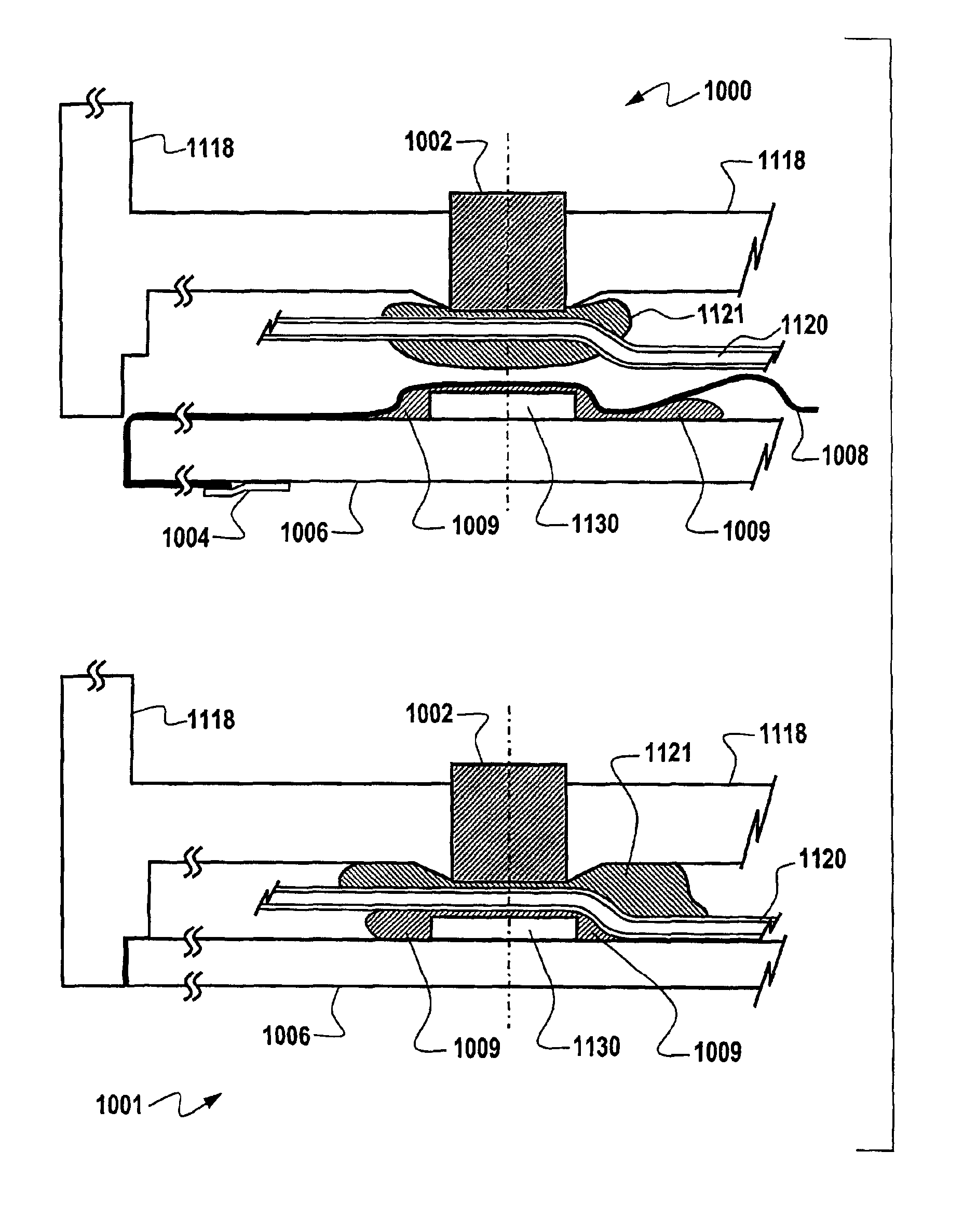
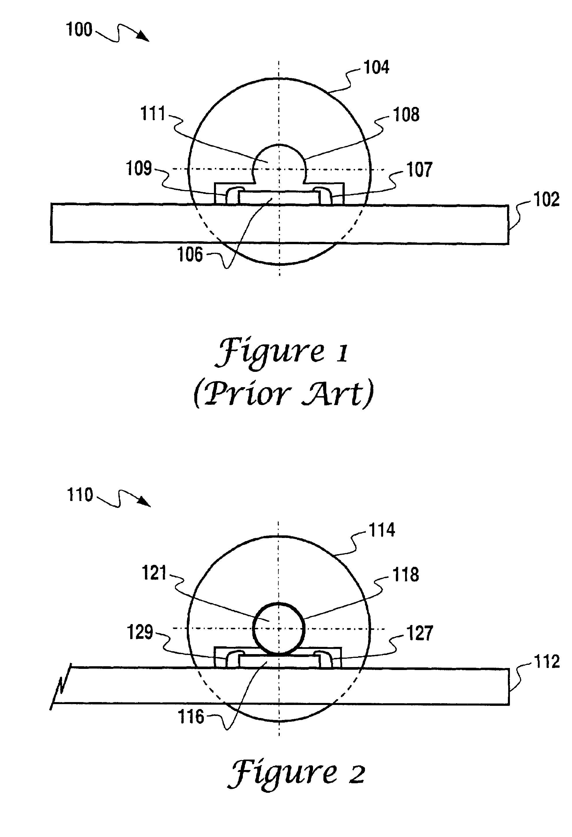
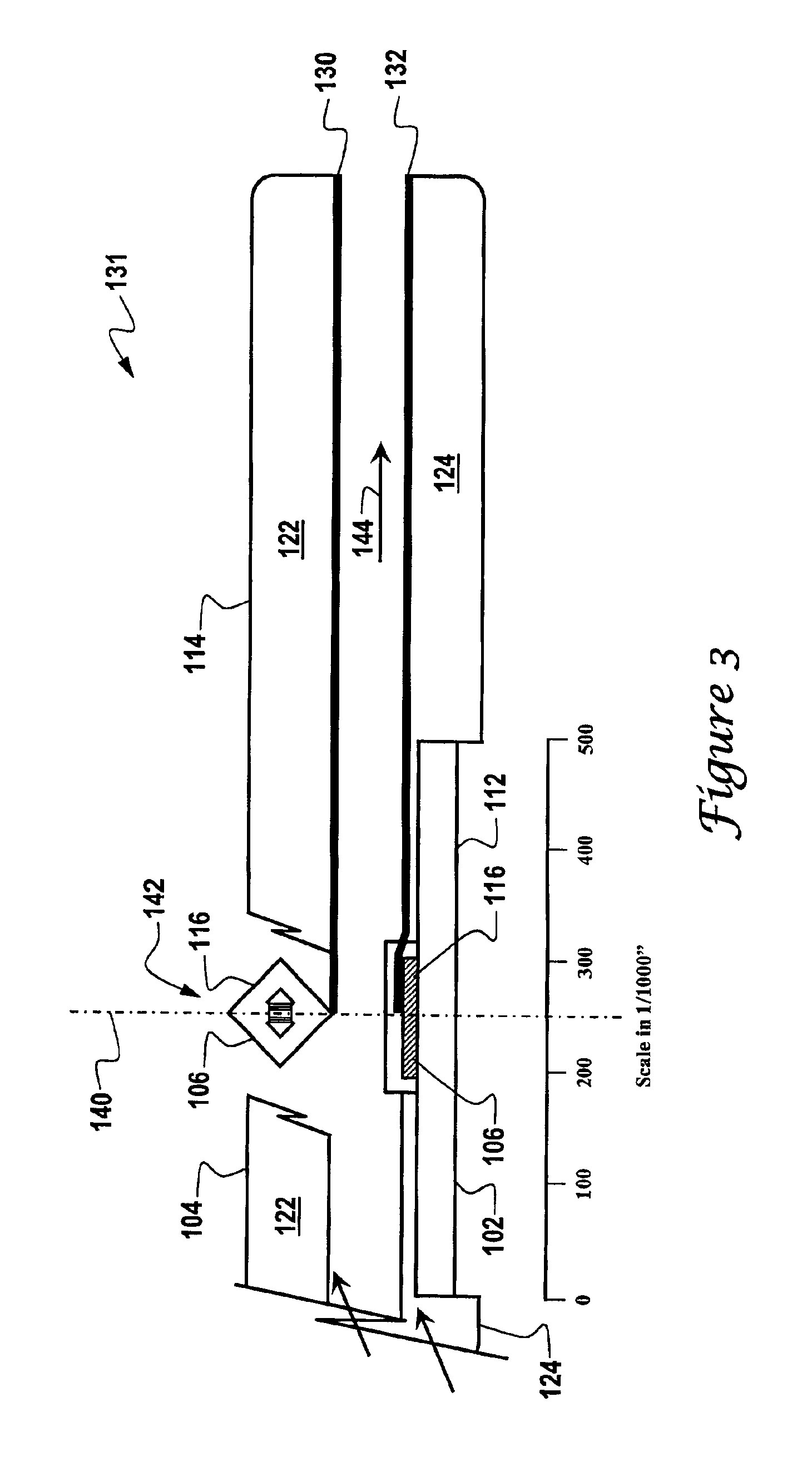
[0035]The present invention is related to the design and fabrication of the electrical insulation for electrical contacts to sensor chips using either front-wire-bond (FWB) or through-the-wafer (TTW) contacts of certain thermal flow microsensors or of environmental sensors in general. The present inventors previously insulated Au-wires and Au-pads of FWB sensor chips via materials, such as, for example, dip-coatings, dip-coatings with or without alumina thin-film undercoating, Si3N4, flowable sealants, solvent-resistant sealant with fluoro-silicon, and epoxies. Insulation based on such materials has been attempted as defined generally by the resistances between the sensing elements and the liquid (e.g., salt water) in a flow tube. Such resistance...


PUM

PropertyMeasurementUnit
resistanceaaaaaaaaaa
resistancesaaaaaaaaaa
temperatureaaaaaaaaaa

Abstract

A sensor can be configured to generally include a flow channel block having a flow channel formed therein, and a sensor chip for sensing fluid flow, wherein a fluid in the flow channel surrounds the sensor chip. Alternatively, the sensor chip can be fastened at one side to a substrate and on another side of the substrate to a core tube inserted into the flow channel. This core tube provides electrical insulation and corrosion protection to the sensor chip, reduces flow noise, (and by the non-intrusive nature of the measurement) essentially eliminates the risk of fluid leakage, and maintains the fluid super-clean and contamination-free while improving structural integrity for the thermal measurements derived from the sensor chip. The use of such a core tube configuration also can protect the sensor from corrosion, radioactive or bacterial contamination, overheating, or freeze-ups. Such a core tube configuration also enables the core tube to be detachable and disposable, without requiring the replacement of the more costly sensor chip with its electronics and calibration.

Description

[0001]This is a continuation-in-part of U.S. patent application Ser. No. 09 / 656,694, filed Sep. 7, 2000, entitled “Robust Fluid Flow and Property Microsensor Made of Optimal Material,” which is a continuation-in-part of U.S. patent application Ser. No. 09 / 207,165, filed Dec. 7, 1998, entitled “Rugged Fluid Flow and Property Microsensor,” now U.S. Pat. No. 6,184,773, and of U.S. patent application Ser. No. 09 / 368,621, filed Aug. 5, 1999, entitled “Microsensor Housing,” now U.S. Pat. No. 6,322,247, which is a Continuation-in-Part of U.S. patent application Ser. No. 09 / 239,125, filed Jan. 28, 1999, entitled “Microsensor Housing,” now U.S. Pat. No. 6,361,206. The content of the foregoing patent applications and patents are hereby incorporated by reference.TECHNICAL FIELD[0002]The present invention relates generally to sensors utilized to detect the quality and movement of fluids, in either gaseous or liquid form. The present invention also relates to thermal sensors of such fluids. The ...

Claims


Application Information

Patent Timeline
Patent Type & Authority Patents(United States)
IPC IPC(8): G01F1/684G01F5/00G01N33/00G01N1/22G01N25/20G01N25/48G01N25/18
CPCG01F1/6845G01F1/6847G01F5/00G01N1/2247G01F1/6842G01N25/488G01N33/0014G01N25/18G01N2001/2285
Inventor BONNE, ULRICHSATREN, ERNEST
Owner HONEYWELL INT INC
Why Eureka
Try Eureka