Non volatile memory

a non-volatile memory and memory technology, applied in static storage, digital storage, instruments, etc., can solve the problems of accidental power supply cutoff, write or erase operation, and inability to read out data stored in a selected memory cell with a high degree of accuracy, and achieve the effect of high degree of reliability

Active Publication Date: 2005-06-28
RENESAS ELECTRONICS CORP
View PDF5 Cites 60 Cited by
  • Summary
  • Abstract
  • Description
  • Claims
  • Application Information

AI Technical Summary

Benefits of technology

[0012]In accordance with the means described above, even when the power-supply cutoff occurs before the write or erase operation is completely terminated and a memory cell in a deplete state is generated, the threshold voltage is increased by a write-back operation carried out thereafter, whereby it is possible to avoid a state in which data of a whole memory block including the memory cell can no longer be read out correctly.
[0013]In accordance with another aspect of the present invention disclosed in this specification, there is provided a configuration of an electrically programmable and erasable non-volatile semiconductor memory such as a flash memory, wherein a flag is provided which notifies an external device of a power-supply cutoff in the course of an operation to write or erase information into or from memory cell employed in the memory in the event of such a power-supply cutoff. It is desirable to provide a function for outputting an address, which was accessed at a time the cutoff of the power supply occurred. By notifying the external device such as a host CPU of such information, the external device is capable of recovering data stored in an area of the memory, which has been damaged by the cutoff of the power supply.
[0014]In accordance with a further aspect of the present invention disclosed in this specification, there is provided a configuration of an electrically programmable and erasable non-volatile semiconductor memory such as a flash memory, wherein an operation currently being executed to write or erase information into or from a memory cell employed in the memory is discontinued and a write-back operation is carried out to change a threshold voltage of the memory cell in a direction of increasing the threshold voltage in the event of a power-supply cutoff in the course of the operation to write or erase information into or from the memory cell, whereas an internal power-supply circuit can be switched from one state to another in dependence on the level of a voltage generated by a power supply so as to allow the write-back operation to be carried out successfully. Typically, the internal power-supply circuit can be switched from one state to another by changing the number of charge-pump stages. Thus, since the internal power-supply circuit generates an operating voltage serving as a countermeasure for a decrease in power-supply voltage due to a cutoff of the power supply, the write-back operation can be carried out with a high degree of reliability even in the event of such a power-supply cutoff.

Problems solved by technology

In the case of a flash memory used in a memory card or the like, however, the power supply may be cut off accidentally in the course of a write or erase operation due to an interruption of the power supply or a withdrawal of the memory card from its slot by a user.
As a result, there is generated a deplete-state failure making it impossible to read out data stored in a selected memory cell with a high degree of accuracy.
If a block including a memory cell in which a deplete failure has occurred is used as a system area for storing information of importance to the system employing the flash memory, it is feared that the system is no longer capable of recognizing the memory and, as a result, the system is not capable of carrying out operations normally anymore.

Method used


Image

  • Non volatile memory
  • Non volatile memory
  • Non volatile memory

Examples


Embodiment Construction

[0041]Preferred embodiments of the present invention are explained by referring to diagrams as follows.

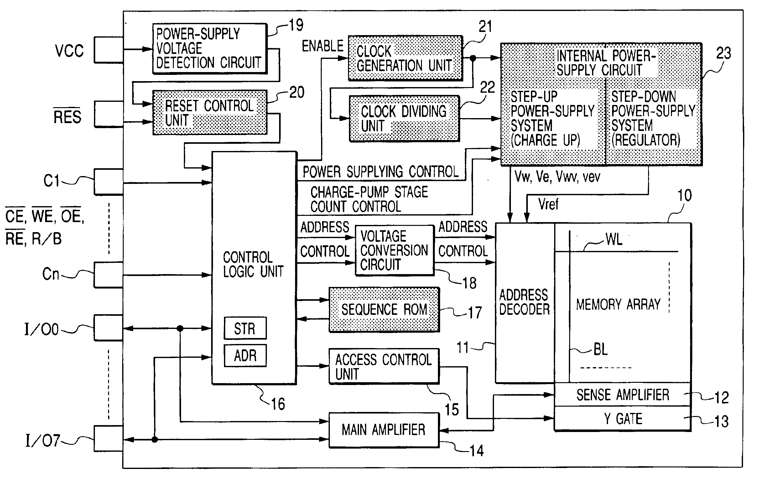
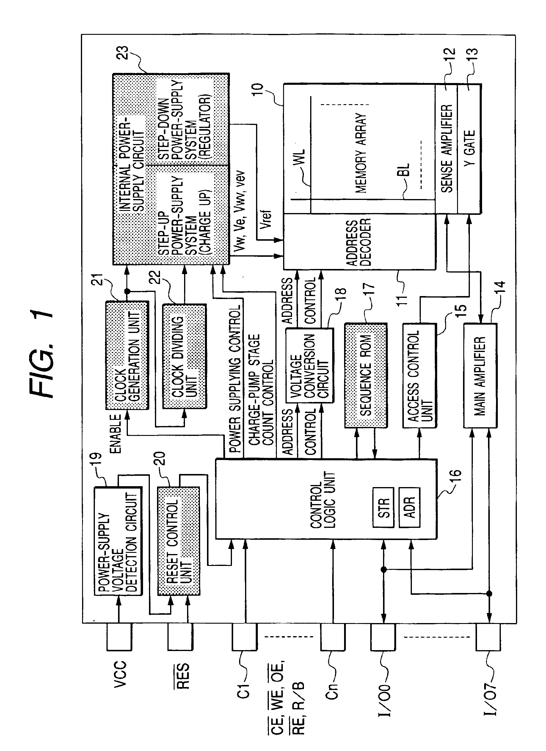
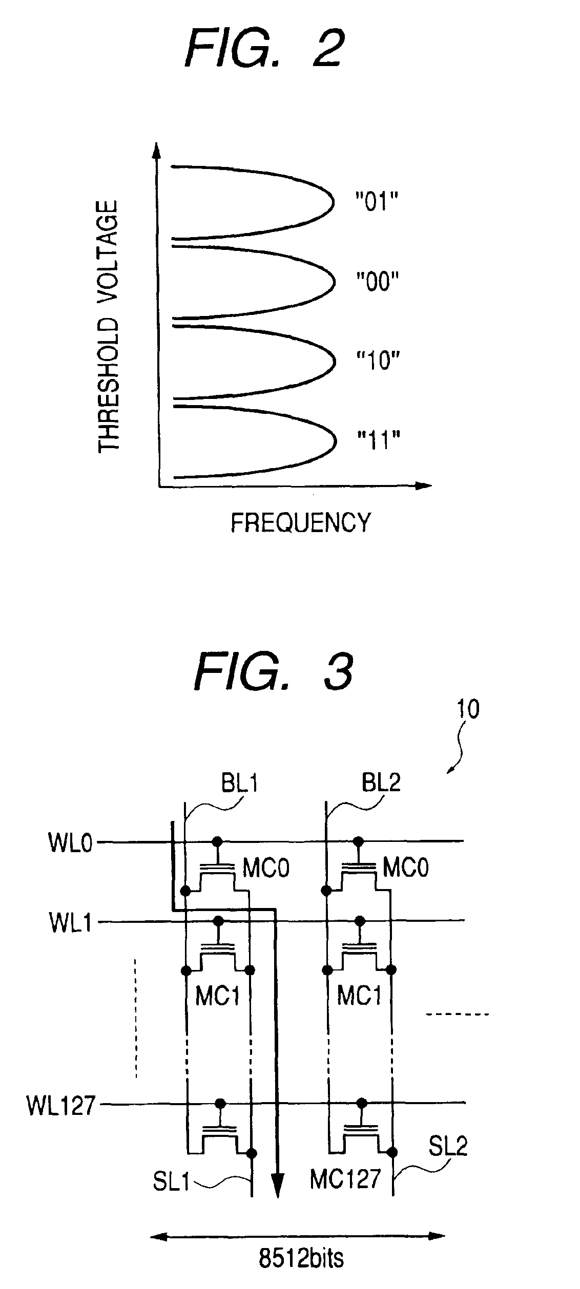
[0042]FIG. 1 is a block diagram showing an embodiment implementing a flash memory used as a typical effective non-volatile semiconductor memory by application of the present invention. In general, a flash memory is a binary memory in which 1 memory cell can be used for storing 1 bit of data. However, the flash memory implemented by this embodiment is a tetranary (4-value) memory in which 1 memory cell can be used for storing 2 bits of data. This flash memory is formed on a semiconductor chip such as single crystal silicon.

[0043]In FIG. 1, reference numeral 10 denotes a memory area in which a plurality of non-volatile memory cells is laid out to form a matrix. Reference numeral 11 denotes an address decoder for decoding an address (X address) signal to select a word line WL in the memory area 10 and set the selected word line WL at a selected-state level. The address decoder 11 incl...


PUM


Abstract

An electrically programmable and erasable nonvolatile semiconductor memory such as a flash memory is designed into a configuration in which, when a cutoff of the power supply occurs in the course of a write or erase operation carried out on a memory cell employed in the non-volatile semiconductor memory, the operation currently being executed is discontinued and a write-back operation is carried out to change a threshold voltage of the memory cell in the reversed direction. In addition, the configuration also allows the number of charge-pump stages in an internal power-supply configuration to be changed in accordance with the level of a power-supply voltage so as to make the write-back operation correctly executable. As a result, no memory cells are put in deplete state even in the event of a power-supply cutoff in the course of a write or erase operation.

Description

BACKGROUND OF THE INVENTION[0001]In general, the present invention relates to a technology serving as a countermeasure taken in the event of a power-supply cutoff in the course of an operation to write or erase information into or from an electrically programmable and erasable non-volatile semiconductor memory. More particularly, the present invention relates to such a technology effectively applied for example to a flash memory allowing bulk erasure of data stored therein to be carried out in predetermined units.[0002]A flash memory employs a non-volatile storage device in each memory cell thereof. The non-volatile storage device includes a MOSFET having a dual-gate structure comprising a control gate and a floating gate. The amount of electric charge accumulated in the floating gate is varied so as to change a threshold voltage of the MOSFET in order to store information into the memory cell.[0003]In an operation to write or erase information into or from a memory cell of a flash ...

Claims


Application Information

Patent Timeline
Patent Type & Authority Patents(United States)
IPC IPC(8): G11C16/02G11C16/00G11C7/00G11C11/34G11C16/06G11C11/56G11C16/22G11C16/30G11C16/34
CPCG11C16/225G11C16/3409G11C16/3404G11C16/30G11C11/5621G11C16/34
Inventor SAKURAI, RYOTAROTANAKA, HITOSHINODA, SATOSHISHIGEMATSU, KOJI
Owner RENESAS ELECTRONICS CORP
Why Eureka
Try Eureka