Semiconductor memory circuit

Inactive Publication Date: 2005-07-05
PANASONIC CORP
View PDF4 Cites 25 Cited by
  • Summary
  • Abstract
  • Description
  • Claims
  • Application Information

AI Technical Summary

Benefits of technology

[0031]Then, the second and third transistors can be disposed at both sides of the second planar capacitor, and the portions connected to the second and third transistors can have a similar shape as the

Problems solved by technology

Nevertheless, it is difficult to decrease the threshold voltage of MOS transistors in proportion to the lowering of the power supply voltage because of variations caused in fabrication processes.
In that case, activating the sense amplifier 102 would not produce a sufficient potential difference between the gate and source of those transistors, causing the sense amplifier 102 to be significantly delayed in, or become incapable of, performing sensing operation for the bit line pair BL and BLX.
Moreover, the numerous memory cells connected to the word line WL make the word line WL h

Method used


Image

  • Semiconductor memory circuit
  • Semiconductor memory circuit
  • Semiconductor memory circuit

Examples


first embodiment

[0050](First Embodiment)

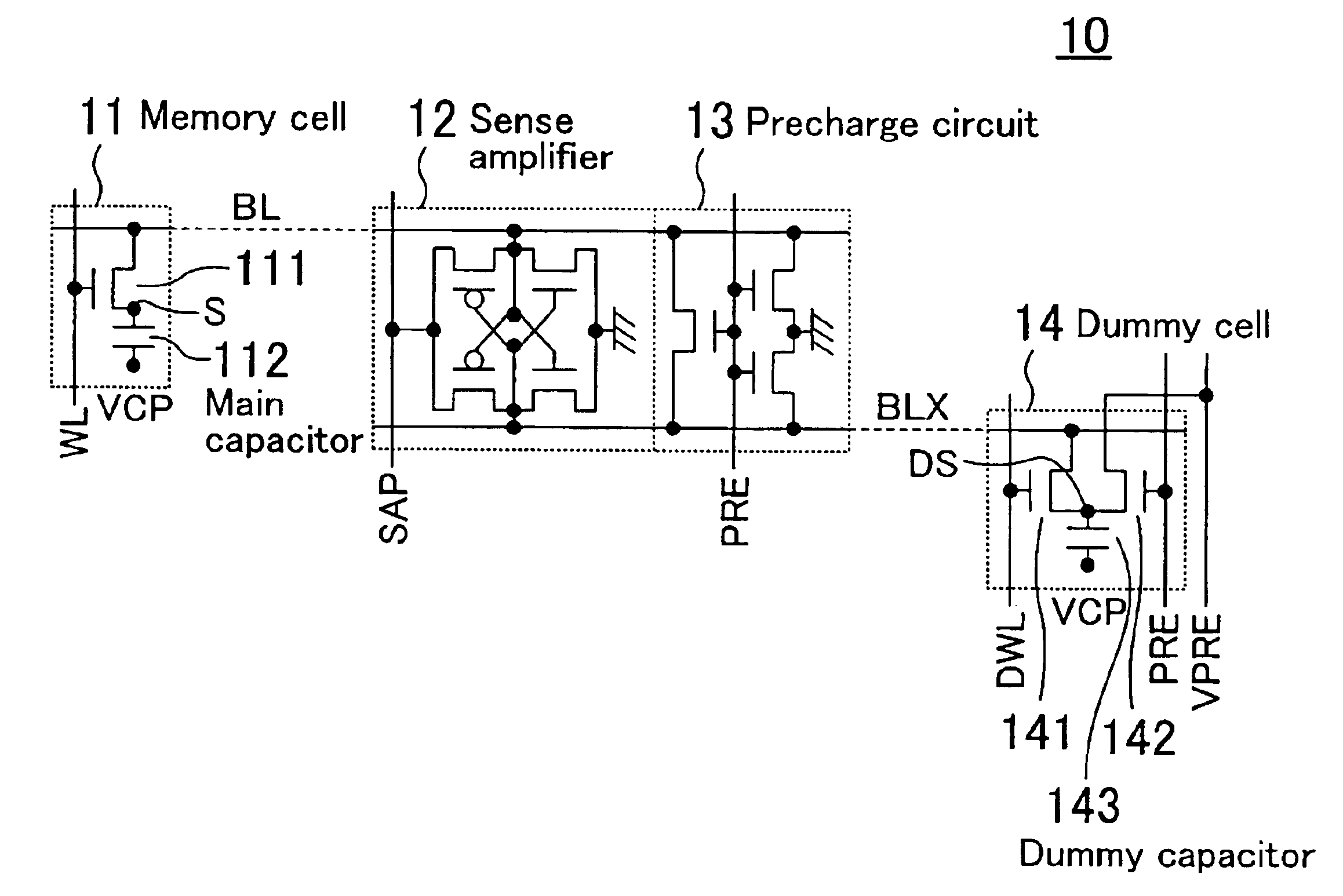
[0051]FIG. 1 illustrates the circuit configuration of a semiconductor memory circuit in accordance with a first embodiment of the present invention. The semiconductor memory circuit of this embodiment, a DRAM 10 of NMOS type, includes a memory cell 11, a CMOS sense amplifier 12, a precharge circuit 13, and a dummy cell 14. The memory cell 11 is at the intersection of a word line WL and a bit line BL. The CMOS sense amplifier 12 serves to sense and amplify a potential difference between the pair of bit lines BL and BLX. The precharge circuit 13 precharges the bit line pair BL and BLX. The dummy cell 14 is provided at the intersection of a dummy word line DWL and the bit line BLX.

[0052]The memory cell 11 is a 1-transistor cell composed of an NMOS transistor 111 and a main capacitor 112. The NMOS transistor 111 is turned on by activating the word line WL while the bit line BL is inactive, thereby electrically connecting the main capacitor 112 to the bit line BL....

second embodiment

[0074](Second Embodiment)

[0075]FIG. 8 illustrates the circuit configuration of a semiconductor memory circuit in accordance with a second embodiment of the present invention. The semiconductor memory circuit of this embodiment, a DRAM 20 of PMOS type, includes a memory cell 21, a CMOS sense amplifier 22, a precharge circuit 23, and a dummy cell 24. The memory cell 21 is at the intersection of a word line WL and a bit line BL. The CMOS sense amplifier 22 serves to sense and amplify a potential difference between the pair of bit lines BL and BLX. The precharge circuit 23 precharges the bit line pair BL and BLX. The dummy cell 24 is provided at the intersection of a dummy word line and the bit line BLX.

[0076]The memory cell 21 is a 1-transistor cell composed of a PMOS transistor 211 and a main capacitor 212. The PMOS transistor 211 is turned on by activating the word line WL when the bit line BL is inactivated, thereby electrically connecting the main capacitor 212 to the bit line BL.

[...


PUM


Abstract

Data reading speed of a DRAM is enhanced without causing an increase in the power consumption and in the chip area. To that end, when data is read, a pair of bit lines is precharged to a GND level, while a dummy cell is charged at a power supply voltage. Immediately after a word line and a dummy word line are activated and their respective potentials are increased by the threshold voltage of an access transistor, a main capacitor and a dummy capacitor are electrically connected to the bit lines, thereby allowing the data to fade in. The resultant potential difference between the pair of bit lines is detected and amplified by a sense amplifier, thereby enabling the data to be read. The capacitance of the dummy capacitor is about half of that of the main capacitor, so that the dummy capacitor can be precharged at the power supply voltage.

Description

BACKGROUND OF THE INVENTION[0001]The present invention relates to semiconductor memory circuits, and more particularly relates to memory access techniques with respect to dynamic memories.[0002]Among the semiconductor memory circuits, dynamic random-access memories (hereinafter referred to as “DRAMs”) have been widely used as devices capable of reading and writing a large amount of data. FIG. 12 illustrates the circuit configuration of a typical DRAM which is currently in practical use. The DRAM 100 shown in FIG. 12 includes a memory cell 101, a sense amplifier 102, and a precharge circuit 103. Hereinafter, referring to a timing chart shown in FIG. 13, how the DRAM 100 reads data will be described.[0003]First, the precharge circuit 103 is activated (PRE=“H”) when the memory cell 101 is inactive (WL=“L”), so that a pair of bit lines BL and BLX (hereinafter referred to as a “bit line pair BL and BLX”) is precharged to a voltage VDD / 2 (VDD is a power supply voltage.) The precharge circ...

Claims


Application Information

Patent Timeline
IPC IPC(8): G11C7/12G11C7/00G11C7/14G11C11/4094G11C11/409G11C11/4099H01L27/108G11C11/401H01L21/8242
CPCG11C7/12G11C7/14G11C11/4094G11C11/4099H01L27/10897H10B12/50
Inventor AGATA, MASASHI
Owner PANASONIC CORP
Why Eureka
Try Eureka