Contact structure and production method thereof and probe contact assembly using same

Inactive Publication Date: 2005-07-12
ADVANTEST CORP
View PDF12 Cites 72 Cited by
  • Summary
  • Abstract
  • Description
  • Claims
  • Application Information

AI Technical Summary

Benefits of technology

[0044]According to the present invention, the contact structure has very high capabilities in various aspects to meet the test requirements of the next generation semiconductor technology. The cantilever contactors are easily and securely mounted on the contactor carrier in the diagonal through holes. The cantilever contactor has a simple shape with a straight and short diagonal beam, an upper beam of which is secured in the diagonal through hole of the contactor carrier and the lower beam is projected from the contactor carrier and functions as a spring, resulting in a high spring rate, high pitch and pin count, high frequency range, and high over drive capability. Because of the probe contact assembly incorporating the contact structure of the present invention is formed by

Problems solved by technology

The conventional technology shown in FIG. 3 has a drawback in that the size of the zig-zaged spring of the contact limits the pitch or pin count of the contactors.
Further, because the interconnection between the contactors and the probe card, or between the contactors and space transformer (not shown), is done through spring contacts, high reliability of interconnection is unavailable.
Further, because of the relatively complicated structure, it is time consuming to adjust the planarity and alignment of the contact points of the contactors.
The conventional technology shown in FIG. 4 has a

Method used


Image

  • Contact structure and production method thereof and probe contact assembly using same
  • Contact structure and production method thereof and probe contact assembly using same
  • Contact structure and production method thereof and probe contact assembly using same

Examples


Example

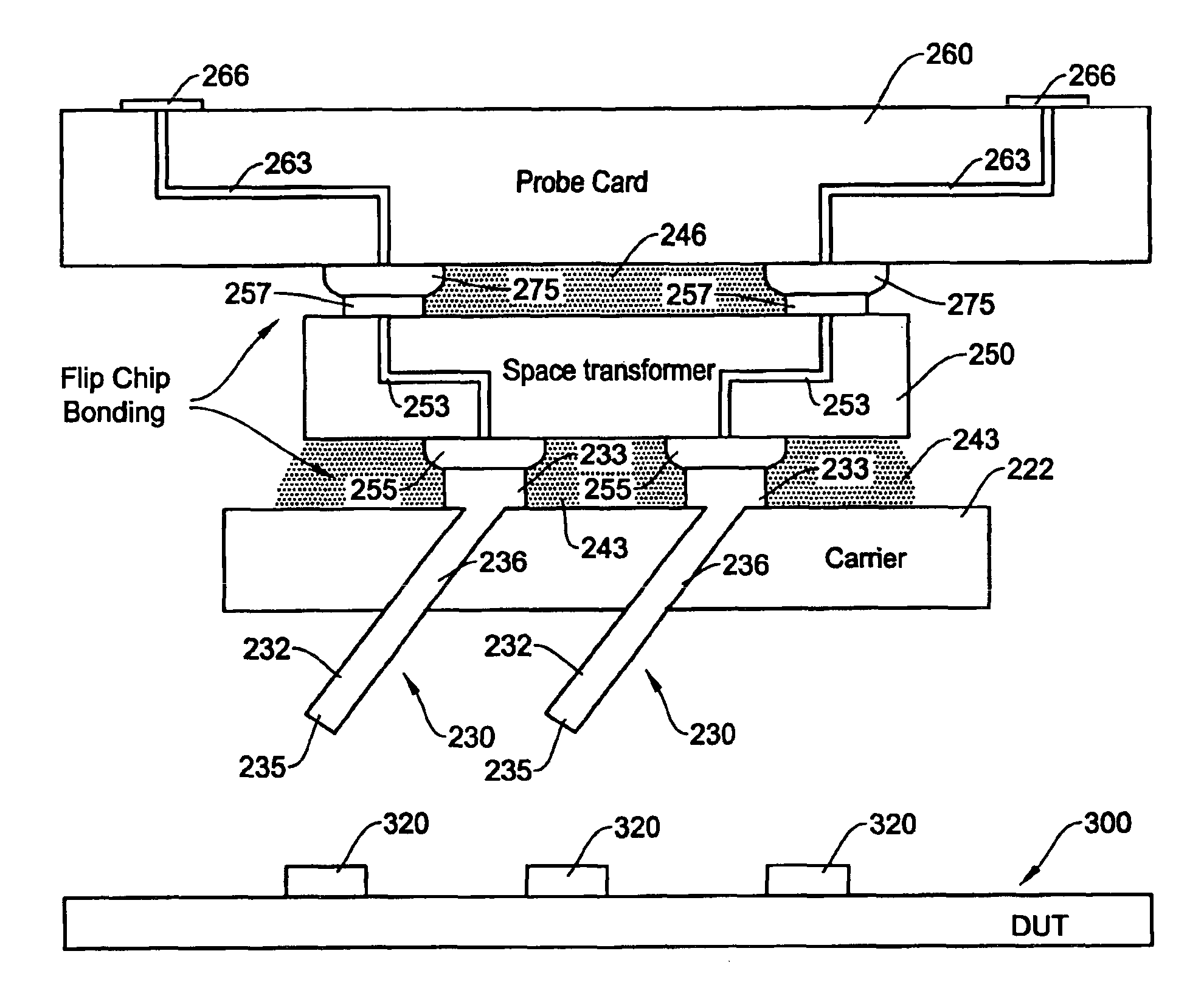
[0073]The present invention will now be explained in detail with reference to the accompanying drawings. FIG. 6 is a cross sectional view showing an example of contact structure of the present invention. The contact structure is configured by a contactor carrier 222, and a plurality of cantilever contactors 230. Each cantilever contactor 230 is extended in the diagonal direction and is mounted in a diagonal through hole of the contactor carrier 222.

[0074]The contactor carrier 222 is made of nonconductive, rigid material such as ceramic, silicon nitride or sapphire. The contactors 230 are made of conductive material such as nickel-cobalt (NiCo) or nonconductive material coated with such conductive material. Although only three contactors are shown, in an actual implementation, a large number of cantilever contactors 230 are mounted on the contactor carrier 222.

[0075]In FIG. 6, each contactor 230 is composed of a top end (base portion) 233 having a flat top surface, a diagonal beam po...


PUM


Abstract

A contact structure for establishing electrical connection with contact targets. The contact structure is formed of a contactor carrier and a plurality of contactors attached to a contactor carrier. The contactors are inserted in diagonal through holes on the contactor carrier and attached to the contactor carrier through adhesives. The contactor has a top end having a flat top surface, a straight diagonal beam integral with the top end and configured by an upper beam portion and a lower beam portion, and a lower end at an end of the lower beam portion to contact with a contact target. A length of the upper beam portion and a length of the lower beam portion are about the same. A probe contact assembly using the contact structure is also disclosed which incorporates a flip chip bonding technology to interconnect the components therein.

Description

[0001]This application claims the benefit of U.S. Provisional Application No. 60 / 417,716 filed Oct. 10, 2002.FIELD OF THE INVENTION[0002]This invention relates to a contact structure and a production method thereof and a probe contact assembly using the contact structure, and more particularly, to a contact structure using a plurality of cantilever contactors mounted on diagonal through holes of a contactor carrier to form a probe contact assembly for testing a semiconductor device, an IC chip, a semiconductor wafer, etc.BACKGROUND OF THE INVENTION[0003]In testing high density and high speed electrical devices such as IC and LSI circuits, a high performance contact structure such as a probe contact assembly having a large number of contactors must be used. The present invention is directed to a contact structure and a probe contact assembly using such a contact structure. The present invention is also directed to a production process of the contact structure and the probe contact as...

Claims


Application Information

Patent Timeline
IPC IPC(8): G01R1/073G01R3/00
CPCG01R1/07378G01R3/00
Inventor ZHOU, YUYU, DAVID
Owner ADVANTEST CORP
Why Eureka
Try Eureka