Microcavity OLED device

a display device and microcavity technology, applied in the direction of discharge tube luminescnet screens, discharge tube/lamp details, electric discharge lamps, etc., can solve the problems of reducing the total luminance integrated over wavelength, complicated structure, and inability to achieve the effect of improving luminance efficiency and color quality

Inactive Publication Date: 2005-07-12
GLOBAL OLED TECH
View PDF7 Cites 110 Cited by
  • Summary
  • Abstract
  • Description
  • Claims
  • Application Information

AI Technical Summary

Benefits of technology

[0010]It is an object of the present invention to provide a microcavity OLED device with improved luminance efficiency and color quality.
[0011]It is a further object of the present invention to provide a microcavity OLED device that can be easily fabricated.
[0012]It is another object of the present invention to provide a microcavity OLED device with a low internal series resistance to reduce the power loss.

Problems solved by technology

A QWS is complicated in structure and expensive to fabricate.
The resonance bandwidth is extremely narrow and, as a result, even though a microcavity based on a QWS is capable of greatly increasing the emission peak height at the resonance wavelength, the total luminance integrated over wavelength is much less improved and can actually decrease over a similar device without the microcavity.
This added conductive electrode layer further complicates the structure.
If a transparent conductive oxide is used as the conductive electrode, the electrical conductance is limited and can be inadequate for many devices especially those having large areas.
If a thin metal film is used, the cavity structure is much more complicated and device performance can be compromised.
QWS-based microcavity OLED devices are therefore not suitable for practical microcavity OLED device applications.
Published attempts to replace the QWS with the more practical metal mirrors have not been very successful.
The authors concluded that the combination of emission dyes with broad emission spectra and a simple planar cavity was not satisfactory for the confinement of light in the microcavity, and encouraged development of new cavity structures.
Although a strong microcavity effect caused emission bandwidth narrowing and a strong angular dependence was observed, no improvement in emission output efficiency was suggested.
However, their performance data showed very little angular dependence characteristic of microcavities.

Method used


Image

  • Microcavity OLED device
  • Microcavity OLED device
  • Microcavity OLED device

Examples


example 1

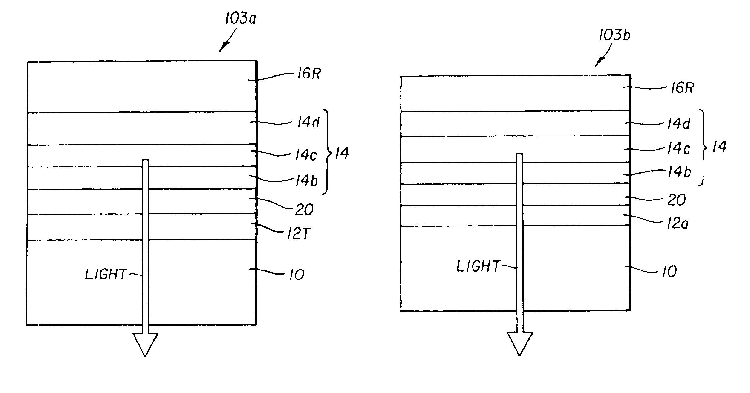
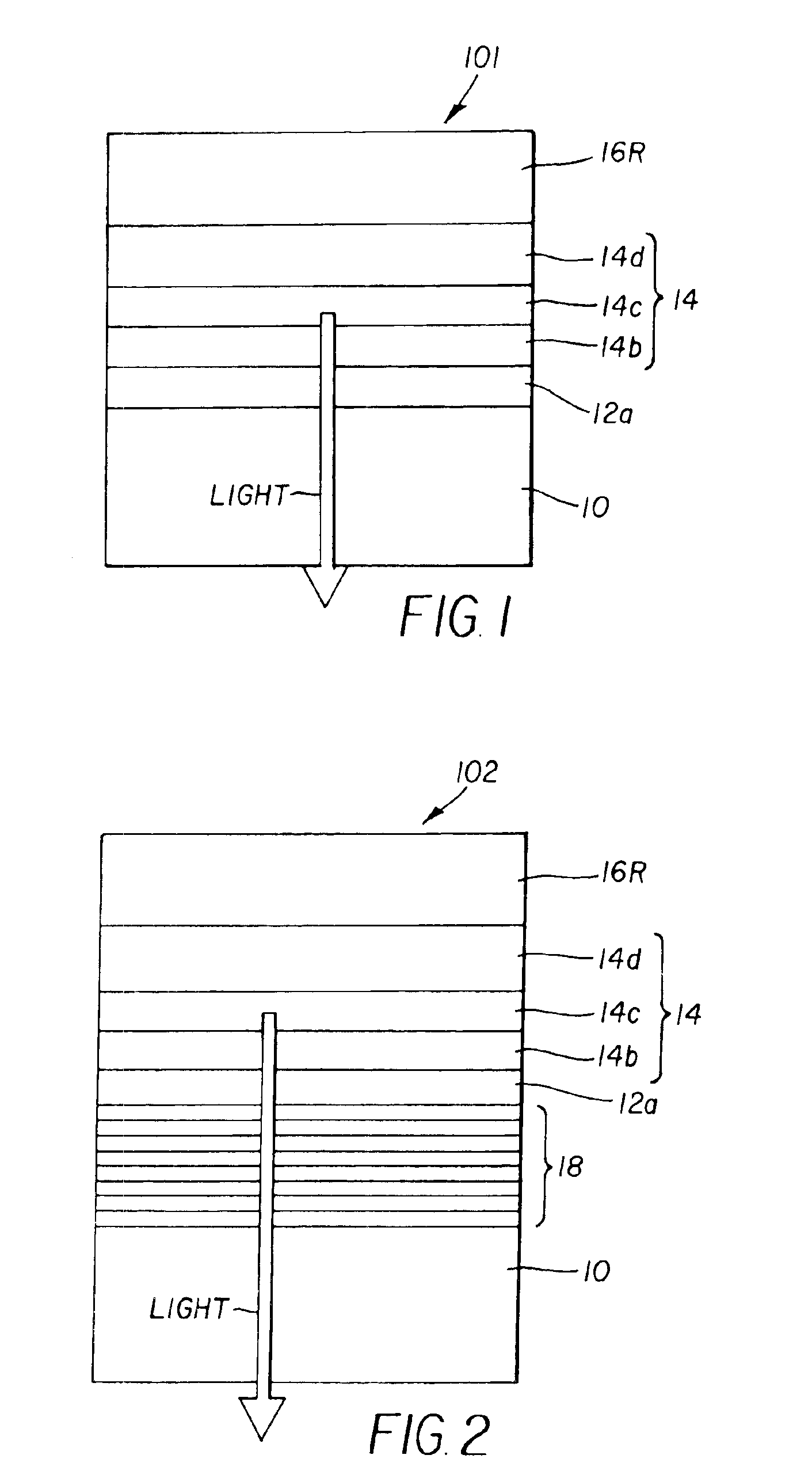
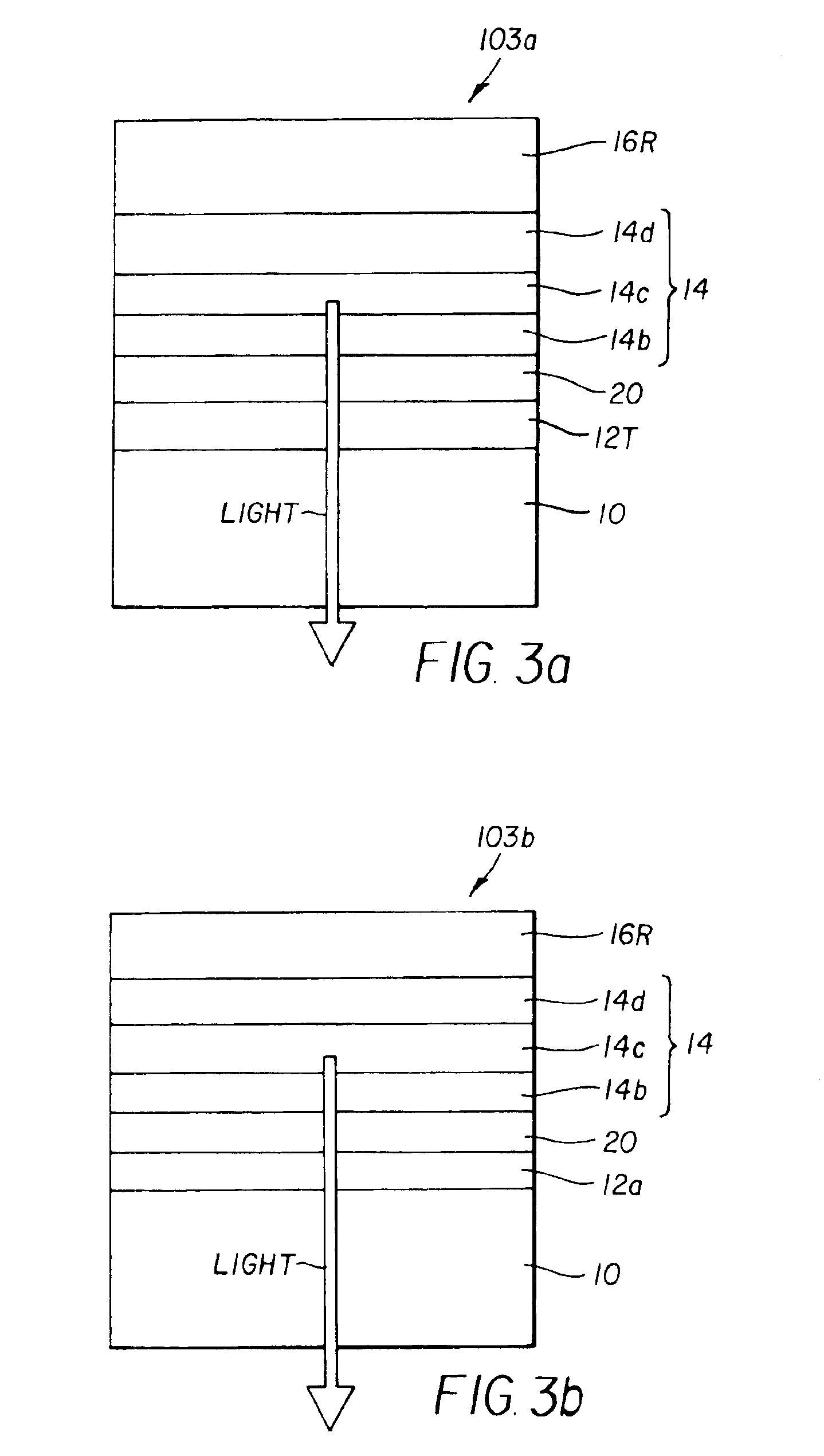
[0126]Example 1 compares the theoretically predicted luminance output of a bottom-emitting microcavity OLED device 103a as shown in FIG. 3A in accordance with the present invention against two comparative devices:

[0127]a) an OLED device 103b without a microcavity, and

[0128]b) a microcavity OLED device 103c using a QWS as one of the mirrors for the microcavity.

[0129]OLED device 103b shown in FIG. 3b was similar in construction to microcavity OLED device 103a except that the light transmissive metallic bottom-electrode 12T which was an Ag anode was replaced by an ITO transparent bottom-electrode 12a. This device represents an OLED device without microcavity, although there is always some optical interference effect in a multi-layer device.

[0130]Microcavity OLED device 103c shown in FIG. 3c was similar in construction to OLED device 103b except that a QWS reflecting mirror 18 was disposed between substrate 10 and ITO transparent bottom-electrode 12a. The QWS reflecting mirror 18 was of...

example 2

[0134]Example 2 is a demonstration of the benefit of the absorption-reducing layer 22 for a bottom-emitting device.

[0135]FIG. 3D illustrates schematically the cross-sectional view of a bottom-emitting microcavity OLED device 103d. Microcavity OLED device 103d was similar in structure to microcavity OLED device 103a except an absorption-reducing layer 22 was disposed between substrate 10 and light transmissive metallic bottom-electrode 12T. For this example, ITO was selected as the absorption-reducing layer 22. Our calculations showed that the effectiveness of the absorption-reducing layer 22 in enhancing luminance output would improve if a higher index of refraction material were used. As will be apparent from Example 4, luminance output could also be increased if the absorption-reducing layer 22 were in direct contact with air rather than with glass. The thickness of all layers was optimized as in Example 1. The results of the calculation are summarized in Table 2. It can be seen t...

example 3

[0137]Example 3 compares the theoretically predicted luminance output of a top-emitting microcavity OLED device 104a in accordance with the present invention against two comparative devices:

[0138]a) an OLED device 104b without a microcavity,

[0139]b) a microcavity OLED device 104c using a QWS as one of the reflecting mirrors for the microcavity.

[0140]FIG. 4A illustrates schematically the cross-sectional view of an exemplary top-emitting microcavity OLED device 104a according to the present invention. Microcavity OLED device 104a included a glass substrate 10, a Ag reflective metallic bottom-electrode 12R, a transparent conductive phase-layer 20, an organic EL medium structure 14, and an Ag light transmissive metallic top-electrode 16T.

[0141]OLED device 104b shown in FIG. 4b was similar in construction to microcavity OLED device 104a except that the Ag light transmissive metallic top-electrode 16T was replaced by an ITO transparent top-electrode 16a which we required to have a thickne...


PUM

PropertyMeasurementUnit
thicknessaaaaaaaaaa
thicknessaaaaaaaaaa
resonance wavelengthaaaaaaaaaa

Abstract

A microcavity OLED device including a substrate; a metallic bottom-electrode layer disposed over the substrate; a metallic top-electrode layer spaced from the metallic bottom-electrode layer; and an organic EL medium structure having a defined thickness, and including a light-emitting layer comprising a host material and at least one dopant disposed between the top-electrode layer and the bottom-electrode layer; wherein one of the metallic electrode layers is light transmissive and the other one is essentially opaque and reflective; wherein the material for reflective metallic electrode layer includes Ag, Au, Al, or alloys thereof, and the material for the light transmissive metallic electrode layer includes Ag, Au, or alloys thereof. The at least one dopant is selected to generate one of red, green, or blue light in the light-emitting layer. The defined thickness of the EL medium structure is selected so that the microcavity OLED device is tuned for emission of one of red, green, or blue light through the light transmissive electrode layer.

Description

CROSS REFERENCE TO RELATED APPLICATIONS[0001]Reference is made to commonly assigned U.S. patent application Ser. No. 10 / 346,424 filed Jan. 17, 2003 entitled “Microcavity OLED Devices” by Yuan-Sheng Tyan et al.; U.S. patent application Ser. No. 10 / 368,513 filed Feb. 18, 2003 entitled “Tuned Microcavity Color OLED Display” by Yuan-Sheng Tyan et al.; U.S. patent application Ser. No. 10 / 356,271 filed Jan. 31, 2003 entitled “Color OLED Display with Improved Emission” by Yuan-Sheng Tyan et al.; and U.S. patent application Ser. No. 10 / 347,013 filed Jan. 17, 2003, entitled “Organic Light Emitting Diode (OLED) Display With Improved Light Emission Using Metallic Anode” by Pranab K. Raychaudhuri et al., the disclosures of which are incorporated herein by reference.FIELD OF INVENTION[0002]The present invention relates to an improved tuned microcavity color OLED display device.BACKGROUND OF INVENTION[0003]Organic electroluminescent (EL) devices or organic light emitting diodes (OLEDs) are electr...

Claims


Application Information

Patent Timeline
Patent Type & Authority Patents(United States)
IPC IPC(8): H01J1/62H01J1/00H01L51/00H05B33/00H01L27/32H01L51/52
CPCH01L27/3211H01L51/5265H10K59/35H10K50/852
Inventor TYAN, YUAN-SHENGFARRUGGIA, GIUSEPPESHORE, JOEL D.DEATON, JOSEPH C.VAN SLYKE, STEVEN A.
Owner GLOBAL OLED TECH
Why Eureka
Try Eureka