System and method of transfer printing an organic semiconductor

a transfer printing and organic semiconductor technology, applied in the direction of diffusion transfer process, thermography, instruments, etc., can solve the problems of relatively low (510sup>2) carrier mobility, less than 100 on/off ratio, and no prior art known to us of semiconducting material transfer

Inactive Publication Date: 2005-07-19
GLOBALFOUNDRIES US INC
View PDF33 Cites 17 Cited by
  • Summary
  • Abstract
  • Description
  • Claims
  • Application Information

AI Technical Summary

Problems solved by technology

However, there is no prior art known to us in which semiconducting materials are transferred to a second substrate in a crystalline form.
The drawback for this compound is that it has relatively low (5×10⁻² cm2.V−1.s.−1) carrier mobility and even much less satisfactory on / off ratio of less than 100.
In addition, because thin films of this polymer are not stable in air and its field-effect characteristics deteriorate on exposure to air, its application as semiconductor becomes less desirable.
The drawback of pentacene is that it is insoluble in common organic solvents and can only be deposited as a thin film by expensive high vacuum and temperature techniques.
The drawback for using this compound as a pentacene precursor is that due to the multi-step synthesis (more than 9 steps), its preparation, especially in large scale is impractical.
In addition, its conversion to pentacene occurs at a relatively high temperature which prevents the use of most plastics as substrates.
The prior art does not disclose the transfer of small molecules using a simple process of thermal transfer to form patterned layers of the small organic molecule semiconductor material in crystalline form on a substrate.

Method used


Image

  • System and method of transfer printing an organic semiconductor
  • System and method of transfer printing an organic semiconductor
  • System and method of transfer printing an organic semiconductor

Examples


Embodiment Construction

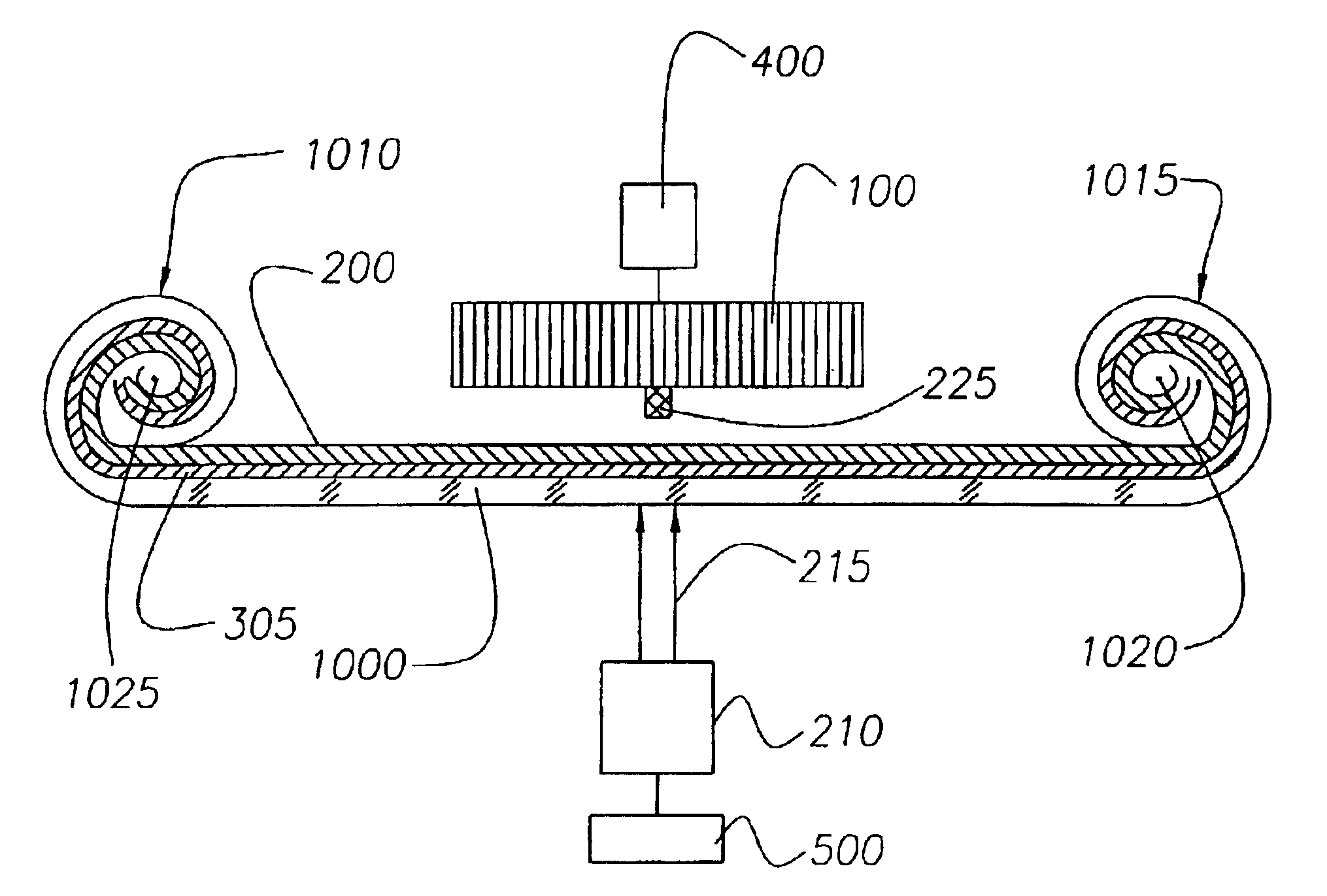
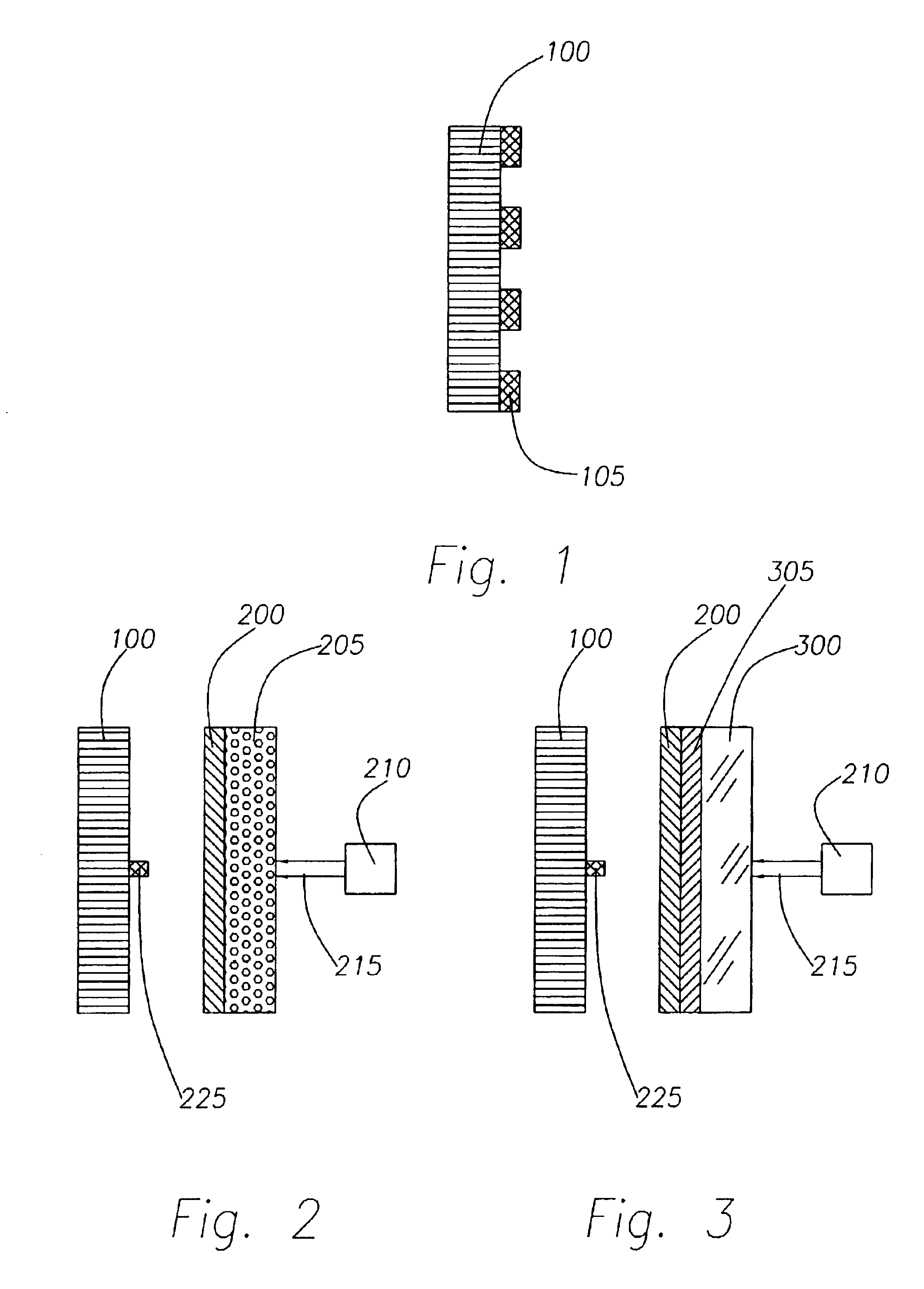
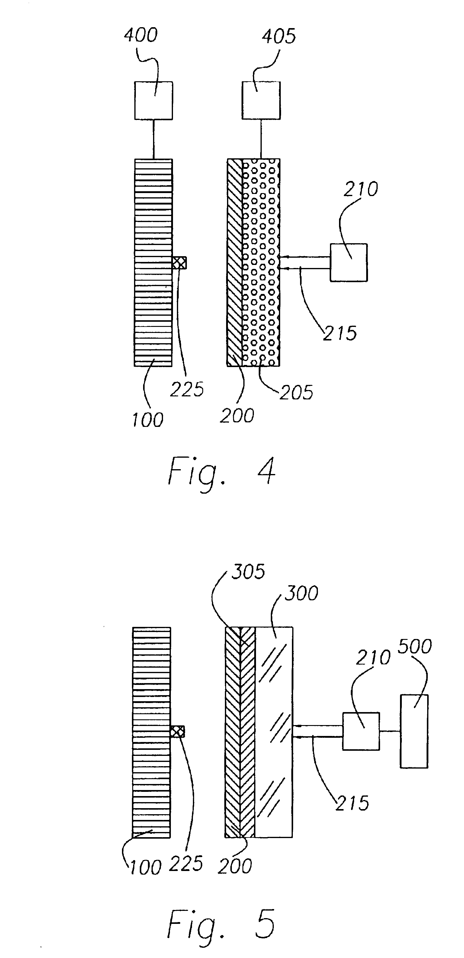
[0044]The present invention provides a substrate having thereon a patterned small molecule organic semiconductor layer having a small organic molecule thermally transferred by exposing a donor substrate having thereon a small molecule organic semiconductor layer to energy.

[0045]The present invention further provides a method of preparing a substrate having thereon a patterned small molecule organic semiconductor layer, involving the exposure of a donor substrate having thereon a small molecule organic semiconductor layer to energy produced from an energy source to cause the thermal transfer of a small organic molecule onto an acceptor substrate to produce a substrate having thereon the patterned small molecule organic semiconductor layer.

[0046]The present invention also provides system for producing a substrate having thereon a patterned small molecule organic semiconductor layer. The system has a donor substrate having thereon a small molecule organic semiconductor layer; an accept...


PUM

PropertyMeasurementUnit
temperatureaaaaaaaaaa
temperaturesaaaaaaaaaa

Abstract

The present invention provides a substrate having thereon a patterned small molecule organic semiconductor layer. The present invention also provides a method and a system for producing a substrate having thereon a patterned small molecule organic semiconductor layer. The substrate having thereon a patterned small molecule organic semiconductor layer is produced by exposing a donor substrate having thereon a small molecule organic semiconductor layer to energy to cause the thermal transfer of a small organic molecule onto an acceptor substrate.

Description

[0001]This application is related to commonly-owned U.S. Application entitled “The Use of an Energy Source to Convert Precursors into Patterned Semiconductors,” Ser. No. 10 / 314,607, filed herewith on the same day, Dec. 9, 2002, cross-referenced and incorporated herein by reference.BACKGROUND OF THE INVENTION[0002]1. Field of the Invention[0003]The present invention relates to substrates having thereon a patterned small molecule organic semiconductor layer. The invention also relates to a method and a system for the production of such substrates having patterned small molecule organic semiconductor layers thereon. The patterned small molecule organic semiconductor layer is formed by the thermal transfer of a small molecule organic semiconductor or its precursor from a donor substrate to an acceptor substrate. More particularly the present invention relates to a substrate having thereon a patterned pentacene semiconductor layer.[0004]2. Description of the Prior Art[0005]The concept of...

Claims


Application Information

Patent Timeline
Patent Type & Authority Patents(United States)
IPC IPC(8): B41M5/26H01L51/40H01L51/05H01L51/30B41M5/382H01L51/00
CPCB41M5/265B41M5/38214H01L51/0013Y10T156/1705H01L51/0044H01L51/0052Y10T428/24802H01L51/0036H10K71/18H10K85/154H10K85/113H10K85/615
Inventor AFZALI-ARDAKANI, ALIHAMANN, HENDRIKCHAUDHARI, PRAVEENVON GUTFELD, ROBERT
Owner GLOBALFOUNDRIES US INC
Why Eureka
Try Eureka