

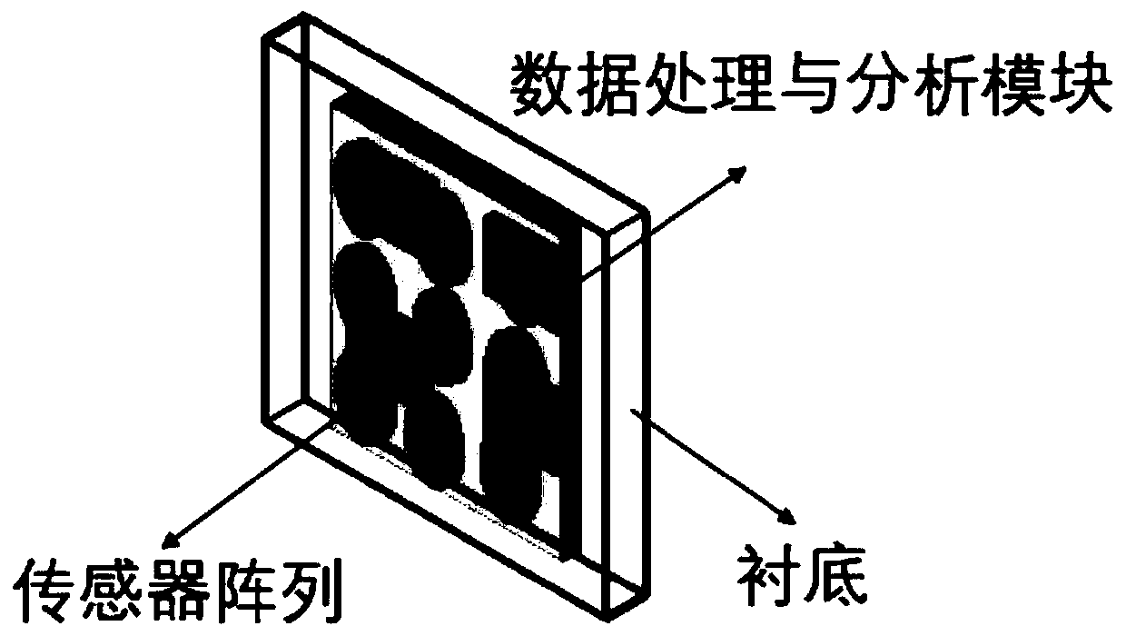
Quantum dot-based electronic nose chip and design method thereof
A design method and technology of quantum dots, applied in measurement devices, instruments, scientific instruments, etc., can solve the problems of low precision, low integration and high power consumption, and achieve the effect of improving the recognition accuracy
- Summary
- Abstract
- Description
- Claims
- Application Information
AI Technical Summary
Problems solved by technology
Method used
Image

Examples
Embodiment 1
[0046] (1) Preparation of SnO 2 quantum dot material. where SnO 2 Quantum dots are made of SnCl 4 ·5H 2 O was used as tin source and synthesized by solvothermal method. Specifically, add 20ml oleic acid, 2.5ml oleylamine, 0.6g SnCl to a 50ml beaker 4 ·5H 2 O, ultrasonically stirred until the SnCl 4 ·5H 2 O is completely dissolved, then add 10ml of ethanol to it, continue ultrasonic stirring until the solution is uniformly dispersed, transfer the mixed solution to a stainless steel reaction kettle, react at 180°C for 8h, and then cool to room temperature through a cold water bath; collect the precipitate, and use Wash several times with absolute ethanol and toluene, disperse in toluene solution to obtain 20mg / ml SnO 2Quantum dot solution. (2) The quantum dot material is coated on the MEMS substrate to form a film by inkjet printing, and a resistive sensor unit is prepared. Based on this sensor unit, a MEMS sensor array is designed and prepared in combination with micro...
Embodiment 2
[0049] (1) Preparation of PbS quantum dot materials. Among them, Pbs quantum dots are synthesized by using PbO as a lead source, TMS as a sulfur source, and thermal injection. Specifically, 1.8 g of lead oxide, 6 mL of oleic acid, and 20 mL of octadecene were stirred in a three-necked flask at high speed, and the temperature of the precursor was raised to 120° C. after vacuuming. In the glove box, 280 uL of TMS was dissolved in 10 ml of octadecene with a pipette gun to prepare sulfur precursors. The sulfur precursor was quickly injected into the lead precursor in a nitrogen environment, reacted for 30 seconds and then placed in a cold water bath for rapid cooling. The precipitate was collected, washed several times with toluene acetone, and dispersed into n-octane solution to obtain a 20 mg / ml PbS quantum dot solution. (2) The quantum dot material is coated on the transistor to form a film by drop coating, and a sensor unit suitable for a field effect transistor is prepared....
PUM
 Abstract
Description
Claims
Application Information