Dual-acceptor-contained three-element solar cell
A technology of solar cells and double acceptors, applied in circuits, photovoltaic power generation, electrical components, etc., can solve the problems of ineffective formation of donor-acceptor phase separation, limitation of short-circuit current density of devices, and limitation of carrier transmission efficiency , to achieve the effect of increasing the light absorption range, increasing the short-circuit current density, and increasing the carrier transport speed
- Summary
- Abstract
- Description
- Claims
- Application Information
AI Technical Summary
Problems solved by technology
Method used
Image

Examples
Embodiment 1
[0021] Embodiment 1 (control group):
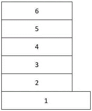
[0022] Clean the substrate composed of transparent substrate and transparent conductive cathode ITO with surface roughness less than 1nm, and blow dry with nitrogen after cleaning; spin-coat ZnO (5000rpm, 40s, 15nm) on the surface of transparent conductive cathode ITO to prepare cathode buffer layer, and bake the formed film (200°C, 60min); prepare P3HT:PC on the cathode buffer layer by spin coating 61 BM (40%:60%) photoactive layer (1000rpm, 25s, 220nm), and baked (140°C, 5min); spin-coated PEDOT:PSS solution on the surface of the photoactive layer to prepare an anode buffer layer (3000rpm, 60s , 30nm); the substrate was annealed by heating and annealing on a constant temperature hot stage (150°C, 5min); metal anode Ag (100nm) was vapor-deposited on the anode buffer layer. Under standard test conditions: AM1.5, 100mW / cm 2 , the open circuit voltage of the device was measured (V OC )=0.56V, short-circuit current (J SC )=8.2mA / cm 2 , ...
Embodiment 2
[0023] Embodiment 2: (control group)
[0024] Clean the substrate composed of transparent substrate and transparent conductive cathode ITO with surface roughness less than 1nm, and blow dry with nitrogen after cleaning; spin-coat ZnO (5000rpm, 40s, 15nm) on the surface of transparent conductive cathode ITO to prepare cathode buffer layer, and bake the formed film (200°C, 60min); prepare PTB7:PC on the cathode buffer layer by spin coating 61 BM (40%:60%) photoactive layer (1200rpm, 60s, 100nm); spin-coat PEDOT:PSS solution on the surface of the photoactive layer to prepare an anode buffer layer (3000rpm, 60s, 30nm); heat the substrate with a constant temperature hot stage Annealing is performed by annealing (150° C., 5 min); metal anode Ag (100 nm) is vapor-deposited on the anode buffer layer. Under standard test conditions: AM1.5, 100mW / cm 2 , the open circuit voltage of the device was measured (V OC )=0.70V, short-circuit current (J SC )=13mA / cm 2 , fill factor (FF)=0.63...
Embodiment 3
[0026] Clean the substrate composed of transparent substrate and transparent conductive cathode ITO with surface roughness less than 1nm, and blow dry with nitrogen after cleaning; spin-coat ZnO (5000rpm, 40s, 15nm) on the surface of transparent conductive cathode ITO to prepare cathode buffer layer, and bake the formed film (200°C, 60min); prepare P3HT:PC on the cathode buffer layer by spin coating 61 BM:PC 71 BM (40%:10%:50%) photoactive layer (1000rpm, 25s, 220nm), and baked (140°C, 5min); spin-coated PEDOT:PSS solution on the surface of the photoactive layer to prepare the anode buffer layer ( 3000rpm, 60s, 30nm); the substrate is annealed by heating and annealing on a constant temperature hot stage (150°C, 5min); metal anode Ag (100nm) is vapor-deposited on the anode buffer layer. Under standard test conditions: AM1.5, 100mW / cm 2 , the open circuit voltage of the device was measured (V OC )=0.56V, short-circuit current (J SC )=9.2mA / cm 2 , fill factor (FF)=0.55, phot...
PUM
| Property | Measurement | Unit |
|---|---|---|
| Thickness | aaaaa | aaaaa |
| Thickness | aaaaa | aaaaa |
| Thickness | aaaaa | aaaaa |
Abstract
Description
Claims
Application Information