Tunnel junctions for long-wavelength vcsels

a technology of vertical cavity and tunnel junction, which is applied in the direction of lasers, semiconductor devices, semiconductor lasers, etc., can solve the problems of non-uniform current injection, high free carrier absorption in the p-doped layer of the laser, and increase the cost of laser power supply, etc., and achieve excellent tunnel junction

Active Publication Date: 2005-11-17
THORLABS QUANTUM ELECTRONICS
View PDF1 Cites 11 Cited by
  • Summary
  • Abstract
  • Description
  • Claims
  • Application Information

AI Technical Summary

Benefits of technology

[0029] The present invention teaches the use of C-doped AlGaAsSb as the p-type tunnel junction layer and demonstrated that the combination P++−AlGaAsSb / N++−AlGaInAs makes an excellent tunnel junction. The introduction of Al allows us to decouple the strain from the bandgap in AlGaAsSb and allows additional freedom in the design of a tunnel junction. The introduction of Al also allows us to overcome the deleterious effect of bandtails formed in heavily p-doped semiconductors.

Problems solved by technology

One problem with this approach is the high free carrier absorption in the p-doped layers of the laser.
This problem becomes worse as the lasing wavelength increases to the longer wavelengths of 1.3 or 1.55 microns.
To make matters worse, the poor mobility of the p-type layers results in a non-uniform current injection.
However, the thickness of the strained layer is limited because it creates crystal defects beyond a certain thickness level, resulting in poor performance of devices and poor reliability.
One technical challenge is that a high probability of tunneling is required in tunnel junctions.
Unfortunately, in many materials grown by organometallic chemical vapor deposition (OMCVD), a significant fraction of the carbon acceptors are compensated by hydrogen (H) atoms preventing a high hole concentration.
Therefore, obtaining high p-type doping by OMCVD, the preferred high volume growth technology, has been difficult due to the passivation of acceptors by hydrogen.
However, if the bandgap of each individual tunnel junction layer is too low for the lasing wavelength, optical absorption by the bandgap increases.
Long-term problems in long-wavelength-VCSELs research remain on how to formulate the optimum compositions of the materials of the tunnel junction layers to meet these criteria and to minimize light absorption in the context of other technical and manufacturing challenges.
Other unknown properties, in particular implementations, include difficulties of doping alternative materials such as AlGaInAs with high p-levels using carbon (C) while minimizing hydrogen (H) passivation.
However, other technical and manufacturing challenges still have to be met.
We believe that even tensile strained GaAsSb may have too low a bandgap to be suitable for long-wavelength VCSELS, such as at 1.3 micron, due to the bandtails formed in heavily p-doped semiconductors giving rise to excessive absorption at energies below the intrinsic bandgap.
When the bandgap is not independent of the strain, there is no flexibility to overcome undesired properties of the tunnel junction.
The bandgap of GaAsSb is too narrow and, as a result, it has large optical absorption or loss if GaAsSb is used as part of the tunnel junction.
But, in this case, the bandgap of GaAsSb is about 1.55 um which is not sufficient to prevent excessive absorption in a tunnel junction used in a VCSEL lasing at a wavelength of 1.55 or 1.31 um lasers.
Bandtails are known but their existence in tunnel junction layers used in VCSELs or other devices have not yet been taught.
The same separation between the photon energy of the lasing wavelength and the intrinsic bandgap of the p-layer of the tunnel junction would give rise to too high an absorption of the laser light.
The detailed nature of how the p-doping and n-doping is used with the particular material systems in the tunnel junction of a long-wavelength VCSEL is a critical issue because the resulting structure must perform multiple functions which include providing a low series resistance, funneling of carriers into the active region, and minimizing the effects of free carrier absorption.
These bandtails are not desirable features but something which cannot be avoided and the resultant increased absorption at the lasing wavelength has to be overcome by increasing the intrinsic bandgap of the p-type tunnel junction layer.

Method used


Image

  • Tunnel junctions for long-wavelength vcsels
  • Tunnel junctions for long-wavelength vcsels
  • Tunnel junctions for long-wavelength vcsels

Examples


example 1

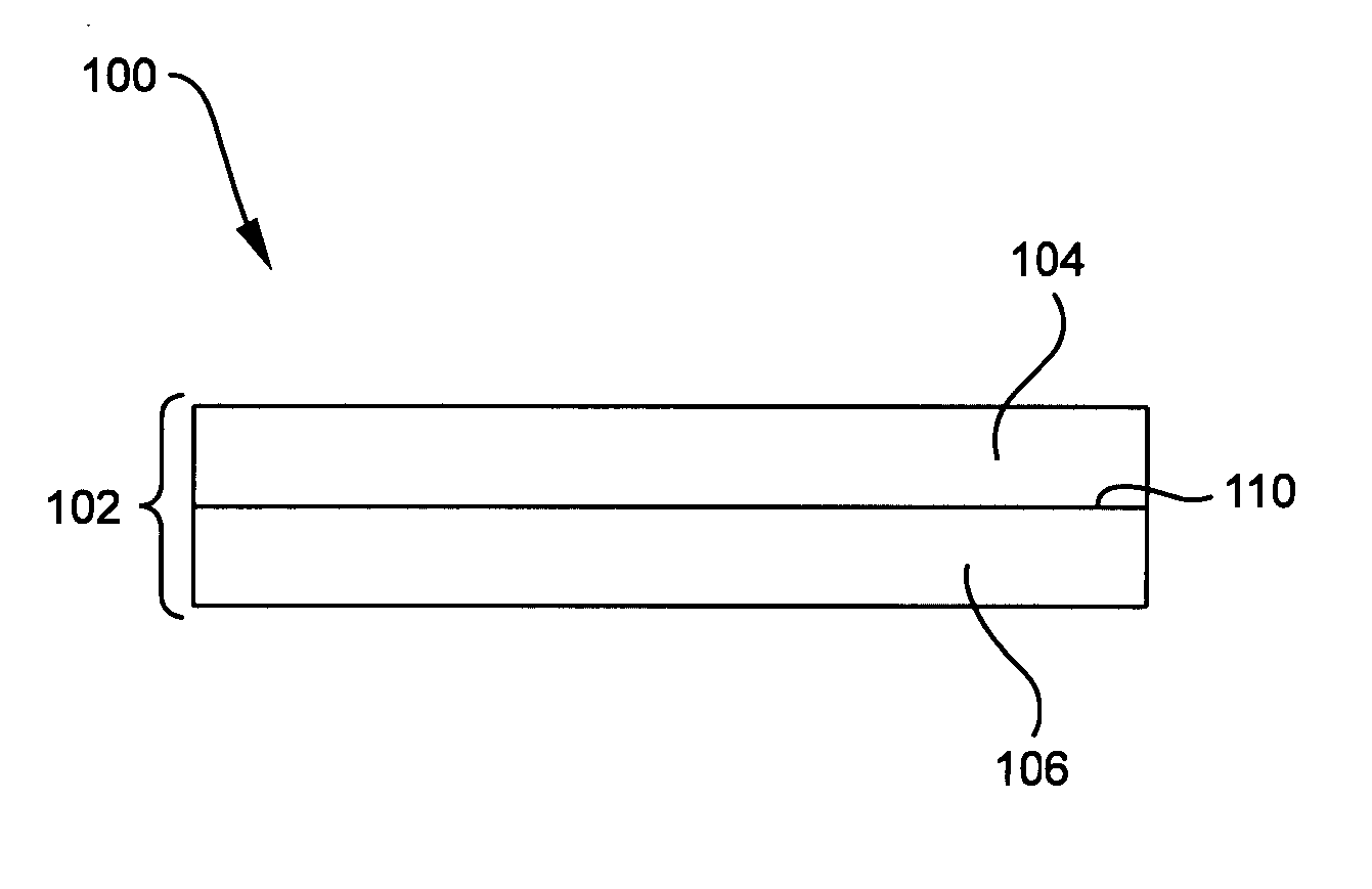
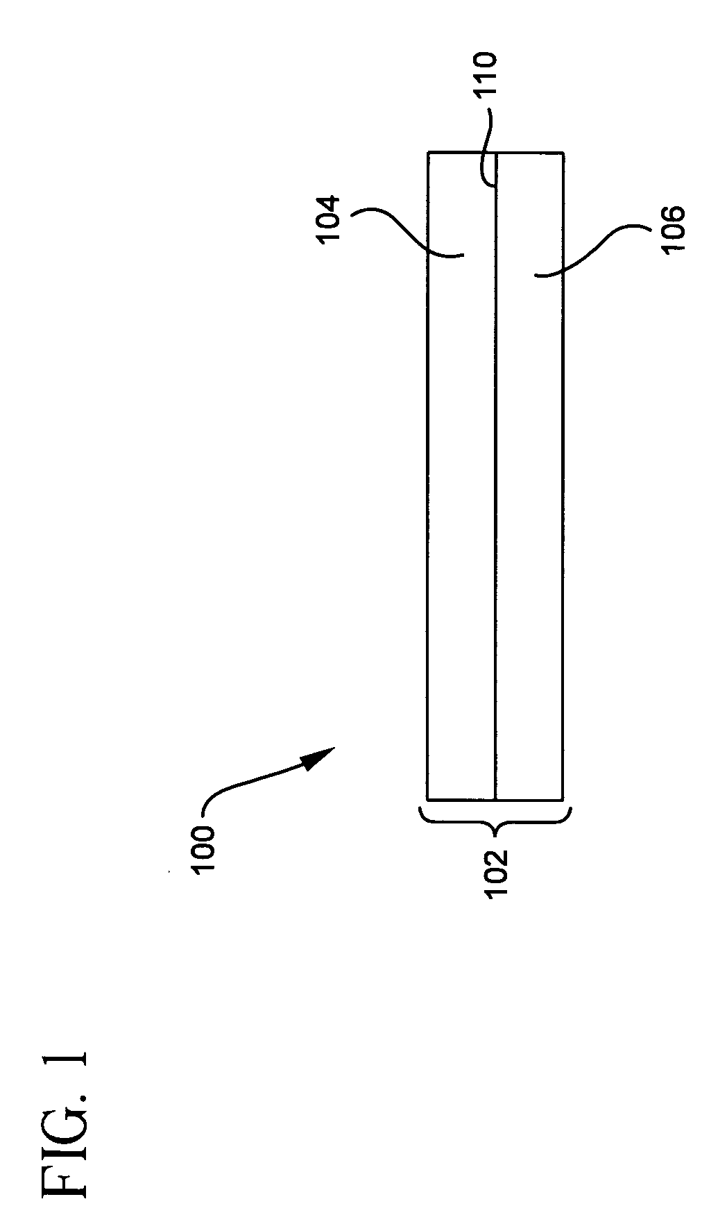
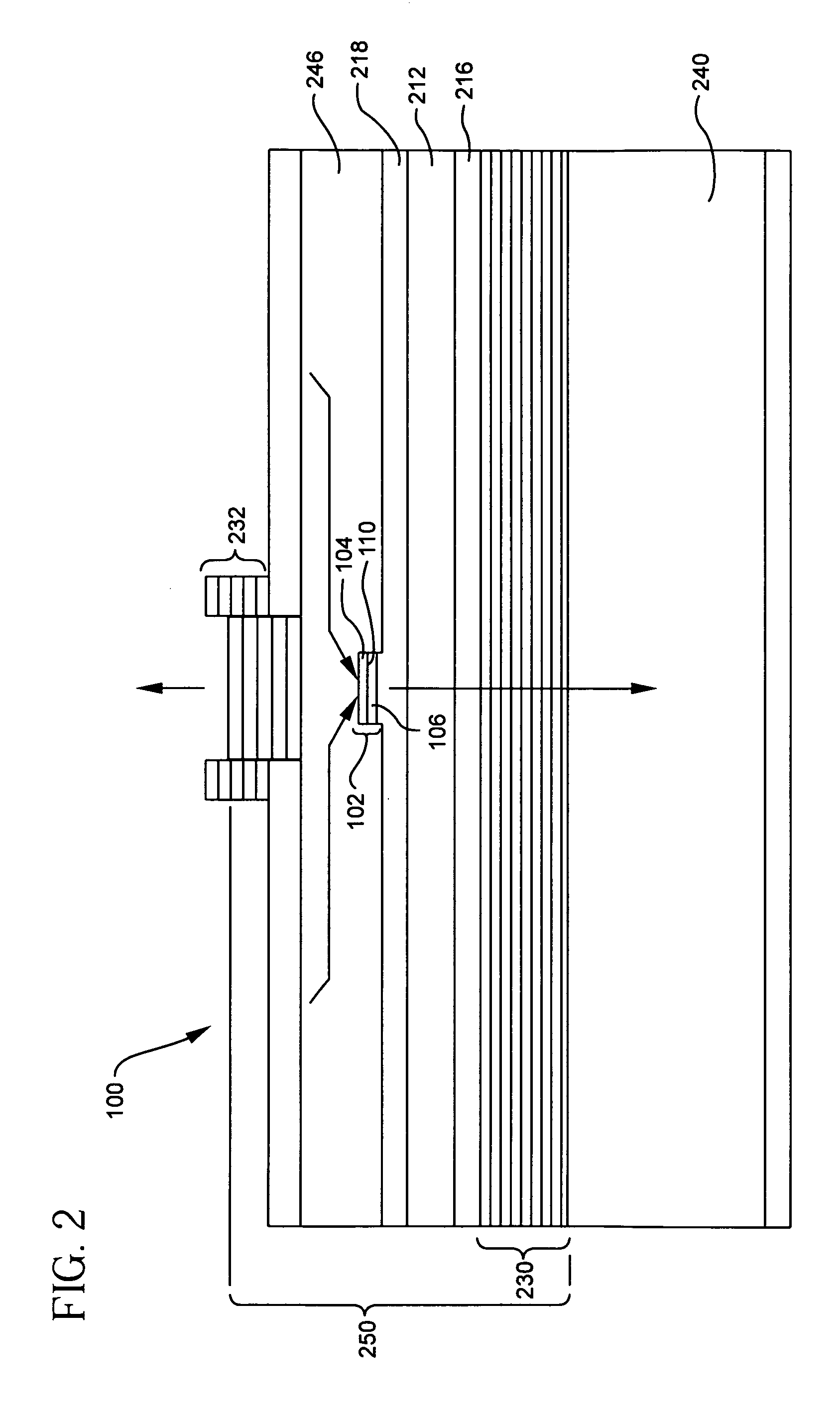
[0074] The band gap of the p-type AlGaAsSb tunnel junction layer 106 can thus be adjusted to a suitable value by adjusting the Al / Ga ratio. The p-type AlGaAsSb layer 106 and the AlGaInAs layer 104 layers may be strained. For 1.3 micron VCSELs the effective bandgap wavelengths of AlGaAsSb and AlGaInAs are selected to be 1.2 microns but other suitable values may also be used, as long as Eq. 1 is satisfied. C-doped AlGaAsSb is grown by OMCVD using suitable precursors such as trimethylaluminum, triethylgallium, arsine, trimethylantimony and carbon tetrabromide. However, any other growth method could be used. Hole concentrations of ˜3×1020 cm−3 have been achieved in AlGaAsSb. The carrier gas was hydrogen and the growth temperature was ˜550° C. A higher growth temperature is preferred in order to minimize hydrogen compensation of the C acceptors. The reagents were trimethylaluminum, triethylgallium, trimethylindium, arsine, phosphine, trimethylantimony, disilane and carbon tetrabromide. T...


PUM


Abstract

A tunnel junction device (102) with minimal hydrogen passivation of acceptors includes a p-type tunnel junction layer (106) of a first semiconductor material doped with carbon. The first semiconductor material includes aluminum, gallium, arsenic and antimony. An n-type tunnel junction layer (104) of a second semiconductor material includes indium, gallium, arsenic and one of aluminum and phosphorous. The junction between the p-type and an-type tunnel junction layers forms a tunnel junction (110).

Description

BACKGROUND OF THE INVENTION [0001] 1. Field of the Invention [0002] The present invention relates generally to surface emitting lasers, and particularly to tunnel junctions for long-wavelength vertical cavity surface emitting lasers (VCSELs). [0003] 2. Technical Background [0004] Vertical cavity surface emitting lasers (VCSELs) have become an important component in data communication systems. Currently commercial lasers operate at 850 nm, where the lasers are made using AlAsGaAs / GaAs semiconductor layers on GaAs substrates. In these lasers the mirrors forming the optical cavity are formed using alternating layers of AlAs and GaAs, with the AlAs / AlGaAs mirror on at least one side of the active region. Adjacent to the active region is an n-type spacer layer, on one side, and a p-type spacer layer, on the other, which inject carriers into the active region when a voltage is applied to the laser. One of the approaches to achieving VCSELs lasing at the important telecommunication wavelen...

Claims


Application Information

Patent Timeline
Patent Type & Authority Applications(United States)
IPC IPC(8): H01L29/205H01S5/183H01S5/30H01S5/323
CPCH01L29/205H01S5/18308H01S5/18358H01S2304/04H01S5/3054H01S5/3095H01S5/3235H01S5/305H01S5/183
Inventor BHAT, RAJARAMNISHIYAMA, NOBUHIKO
Owner THORLABS QUANTUM ELECTRONICS
Why Eureka
Try Eureka