Method of manufacturing a substrate having shallow trench isolation

a technology of integrated circuit and substrate, which is applied in the direction of semiconductor/solid-state device manufacturing, basic electric elements, electric devices, etc., can solve the problems of difficult annealing at such extremely high temperature, difficult to be constituted reaction tubes, etc., and achieve high integration density and reduce the generation of crystalline defects in the device region

Inactive Publication Date: 2005-07-19
KK TOSHIBA
View PDF21 Cites 15 Cited by
  • Summary
  • Abstract
  • Description
  • Claims
  • Application Information

AI Technical Summary

Benefits of technology

[0012]In the light of the above problems, it is an object of the present invention to provide a structure of a semiconductor substrate which is capable of reducing crystalline defects generated in a devic

Problems solved by technology

Further, although the object of the present invention can be attained even if the buried oxide films are annealed at a higher temperature in excess of 1350° C., such problems arise in this case that an annealing apparatus consisting of a reaction tube,

Method used


Image

  • Method of manufacturing a substrate having shallow trench isolation
  • Method of manufacturing a substrate having shallow trench isolation
  • Method of manufacturing a substrate having shallow trench isolation

Examples


first embodiment

[0064](First Embodiment)

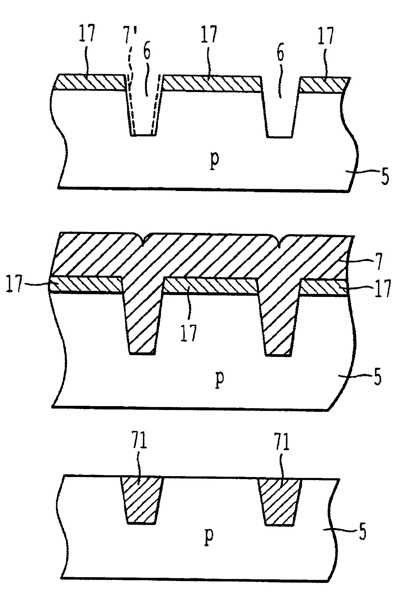
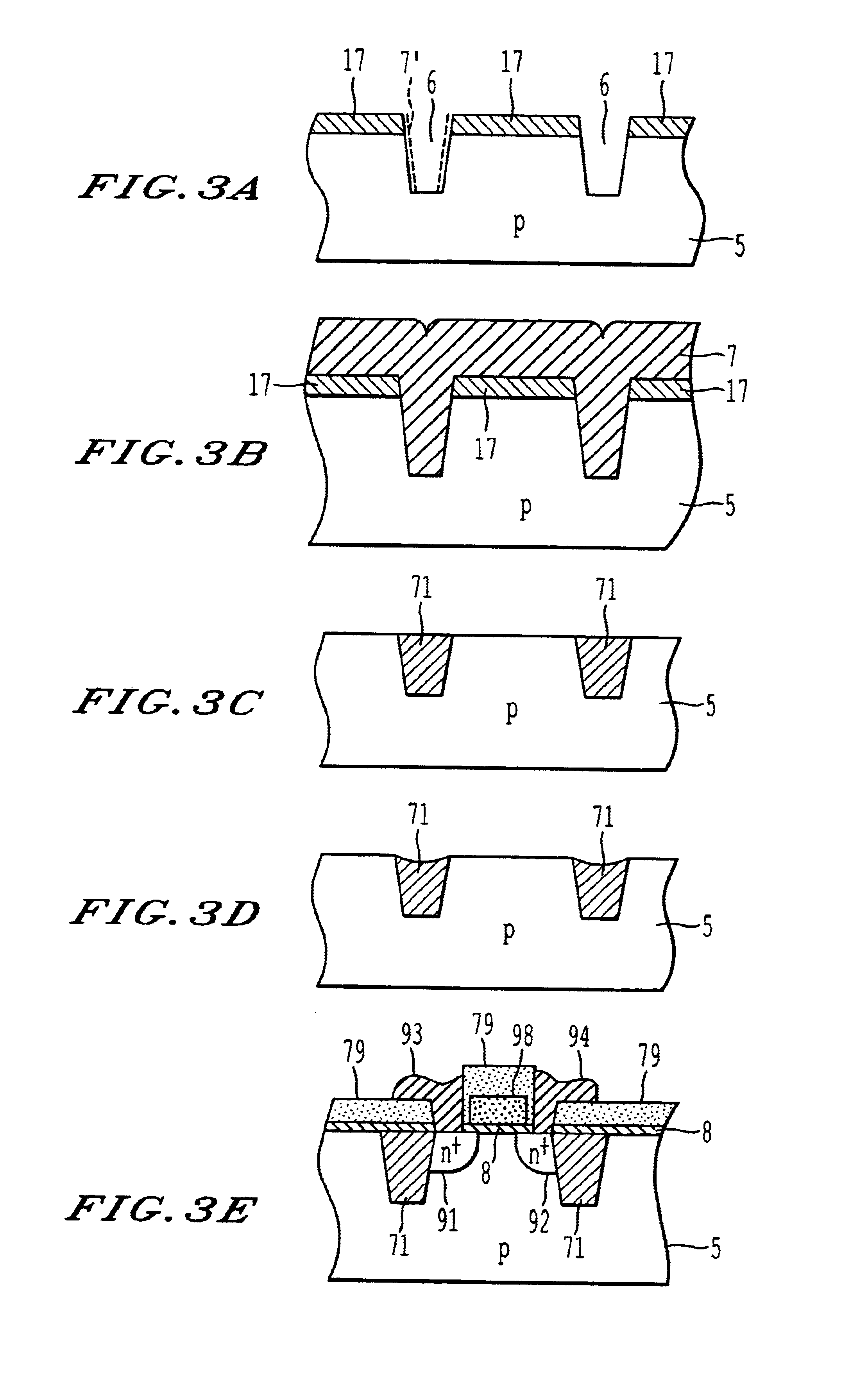
[0065]FIG. 3E shows a sectional structure of buried element isolation semiconductor substrate, or shallow trench element isolation (STI) semiconductor substrate for MOS integrated circuit according to a first embodiment of the present invention. FIGS. 3A to 3D are cross-sectional views showing manufacturing steps to come up to the final structure shown in FIG. 3E. In the element isolation semiconductor substrate according to the first embodiment of the present invention, buried oxide films 71 are formed in the grooves 6 at a surface of the semiconductor substrate 5, as shown in FIG. 3E, and a MOS transistor having an n+ source region 91, an n+ drain region 92, a gate oxide film 8, a polysilicon gate electrode 98, a source electrode 93, a drain electrode 94, and an interlayer insulating film 79 is formed in the device region sandwiched in between the buried oxide films 71, 71.

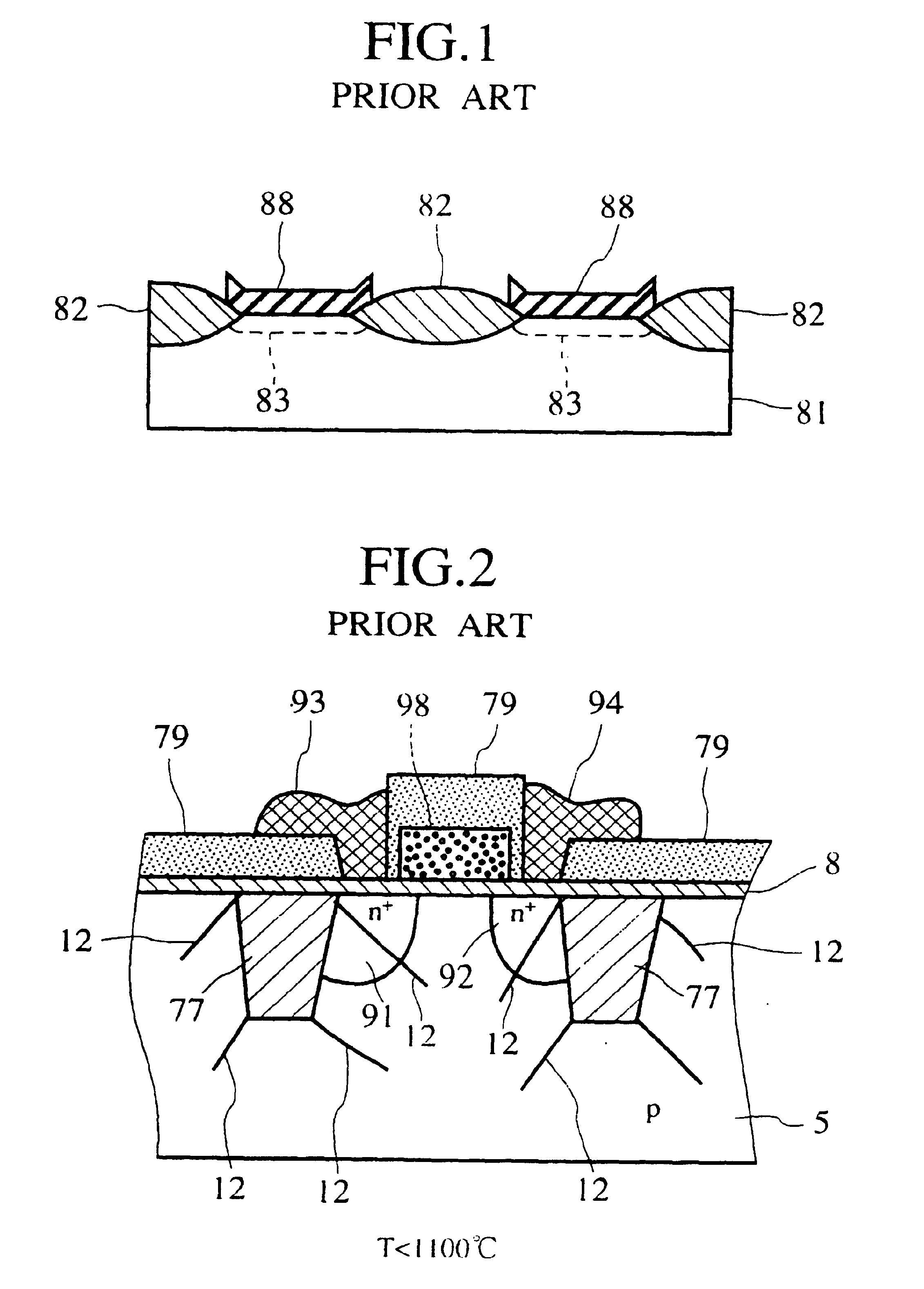
[0066]In the MOS integrated circuit formed in the element isolation semiconductor sub...

second embodiment

[0080](Second Embodiment)

[0081]FIG. 8F is a cross-sectional view showing a structure of an element isolation semiconductor substrate for use in a bipolar integrated circuit according to a second embodiment of the present invention. FIGS. 8A to 8E are schematic cross-sectional views showing steps for manufacturing the semiconductor substrate having the final structure shown in FIG. 8F. A method of manufacturing the element isolation semiconductor substrate for use in the bipolar integrated circuit according to the second embodiment of the present invention comprises following steps.

[0082](a) First, as shown in FIG. 8A, a 200 to 350 nm thick SiO2 film 14 is formed on a surface of a p type silicon substrate 13 by means of steam oxidation.

[0083](b) Then, as shown in FIG. 8B, a surface of part of the silicon substrate 13 is exposed by patterning SiO2 film 14 by virtue of photolithography using photoresist as a mask to form a diffusion mask 14. An n+ buried layer 15 is then formed by ther...

third embodiment

[0089](Third Embodiment)

[0090]FIG. 10G is a cross-sectional view showing a element isolation semiconductor substrate according to a third embodiment of the present invention. FIGS. 10A to 10G are schematic cross-sectional views showing a manufacturing method to achieve the final structure in FIG. 10G. Although a case will be explained in the third embodiment of the present invention where the present invention is applied to a BiCMOS integrated circuit, it is a matter of course that the present invention may be applied to MOS integrated circuit, bipolar integrated circuit, static induction transistor (SIT) integrated circuit, or the like. A method of manufacturing a semiconductor substrate for BiCMOS integrated circuit according to the third embodiment of the present invention will be explained hereinbelow.

[0091](a) First, as shown in FIG. 10A, on a surface of an n type silicon substrate 23 having predetermined face orientation such as (100) face, a 1 μm thick SiO2 film 24 is formed ...


PUM


Abstract

A semiconductor substrate having a shallow trench isolation (STI) structure and a method of manufacturing the same are provided, i.e., an isolation substrate in which grooves are selectively formed at predetermined locations of the semiconductor substrate and oxide films using organic silicon source as material are buried in the grooves as buried oxide films. The present invention is characterized in that the buried oxide films are annealed at a predetermined temperature within the range of 1100 to 1350° C. before or after planarization of the semiconductor substrate such that ring structures of more than 5-fold ring and ring structures of less than 4-fold ring are formed at predetermined rates in the buried oxide films. The above annealing allows stress of the oxide film buried in the grooves to be relaxed. Hence, the generation of dislocation is suppressed.

Description

[0001]This application is a Division of application Ser. No. 08 / 751,438 filed on Nov. 20, 1996, now U.S. Pat. No. 5,994,756.BACKGROUND OF THE INVENTION[0002]1. Field of the Invention[0003]The present invention relates to a substrate for a semiconductor integrated circuit such as LSI and a method of manufacturing the same and, more particularly, to element isolation technique for a semiconductor integrated circuit.[0004]2. Description of the Prior Art[0005]To fabricate an LSI, it is necessary to form element isolation regions for electrically isolating one device region from another device region around respective device regions in which active elements such as transistor or passive elements such as resistor capacitor, etc. are arranged. In the development of MOSLSI technology and bipolar LSI technology, element isolation technique for forming the element isolation region has been always one of important technical themes. Importance of such element isolation technique would be increa...

Claims


Application Information

Patent Timeline
IPC IPC(8): H01L21/762H01L21/70
CPCH01L21/76232H01L21/76264H01L21/76275H01L21/76283
Inventor UMEZAWA, KAORITSUCHIYA, NORIHIKOMATSUSHITA, YOSHIAKIKAMIJOU, HIROYUKIYAGISHITA, ATSUSHIKITA, TSUNEHIRO
Owner KK TOSHIBA
Why Eureka
Try Eureka