Optical path deflecting element, optical path deflecting apparatus, image displaying apparatus, optical element and manufacturing method thereof

a manufacturing method and optical path technology, applied in static indicating devices, instruments, non-linear optics, etc., can solve the problems of difficult to increase the response speed by a sub-microsecond, the optical beam shifter cannot be used in a case where high-speed switching is required, and the size and cost of conventional optical elements are limited. , to achieve the effect of reducing optical noise and resolution, avoiding the increase of size and cost of conventional optical elements and reducing optical nois

Inactive Publication Date: 2005-07-19
RICOH KK
View PDF33 Cites 81 Cited by
  • Summary
  • Abstract
  • Description
  • Claims
  • Application Information

AI Technical Summary

Benefits of technology

[0025]i). Since the pixel shift elements have the complicated structures, it is impossible to avoid an increase in the size an...

Problems solved by technology

Also, the conventional optical elements have limited uses due to the costly materials.
However, in the optical beam shifters according to Japanese Laid-Open Patent Application No. 06-018940, since nematic liquid crystal is used as the liquid crystal material therein, it is difficult to increase the response speed by a sub-microsecond.
As a result, it is impossible to use the optical beam shifters in a case where high-speed switching is required.
Also, in the optical deflection switch according to Japanese Laid-Open Patent Application No. 09-133904, although the ferroelectric liquid crystal of the smectic A phase is used therein, it is impossible to expect high-speed operations because the smectic A phase has no spontaneous polarization.
For instance, since the projection shifting means uses a combination of the optical rotating element and the birefringence element, it is impossible to avoid large loss of the light quantity.
Additionally, a mismatch of the optical rotating element and the birefringence element with respect to the optical characteristics causes optical noise such as a ghost ray due to light leaked in an exterior of a pixel shift, that is, in the place where an image should not be formed.
Additionally, it takes a heavy cost to develop and manufacture these elements in general.
As a result, other problems such as vibration and noise are caused in the projector.
However, when this optical path switching method is adopted in the optical path changing means, the optical path changing means cannot help having a complicated structure for driving an optical element therein.
As a result, it is impossible to avoid high fabrication cost thereof.
However, the optical path shifting means has problems similar to the above-mentioned optical path changing means according to Japanese Laid-Open Patent Application No. 06-324320 in that it is necessary to prepare a comparatively large transparent piezoelectric element and therefore it is impossible to avoid the high fabrication cost thereof.
In general, an optical crystal serving as the birefringence plate is expensive.
Therefore, when an optical crystal corresponding to a size of the illuminant array is used in the optical writer, it is impossible to avoid a cost increase of the optical writer.
According to Japanese Laid-Open Patent Application No. 07-092507, since the optical writer uses the nematic liquid crystal, the optical writer has extremely insufficient response speed of several milliseconds.
If the optica...

Method used


Image

  • Optical path deflecting element, optical path deflecting apparatus, image displaying apparatus, optical element and manufacturing method thereof
  • Optical path deflecting element, optical path deflecting apparatus, image displaying apparatus, optical element and manufacturing method thereof
  • Optical path deflecting element, optical path deflecting apparatus, image displaying apparatus, optical element and manufacturing method thereof

Examples


first embodiment

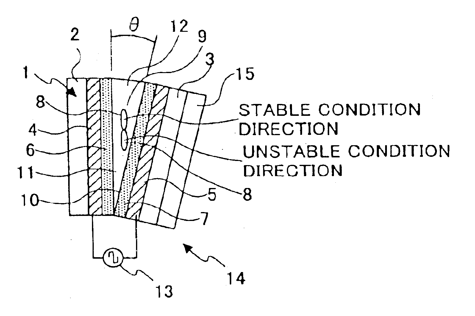
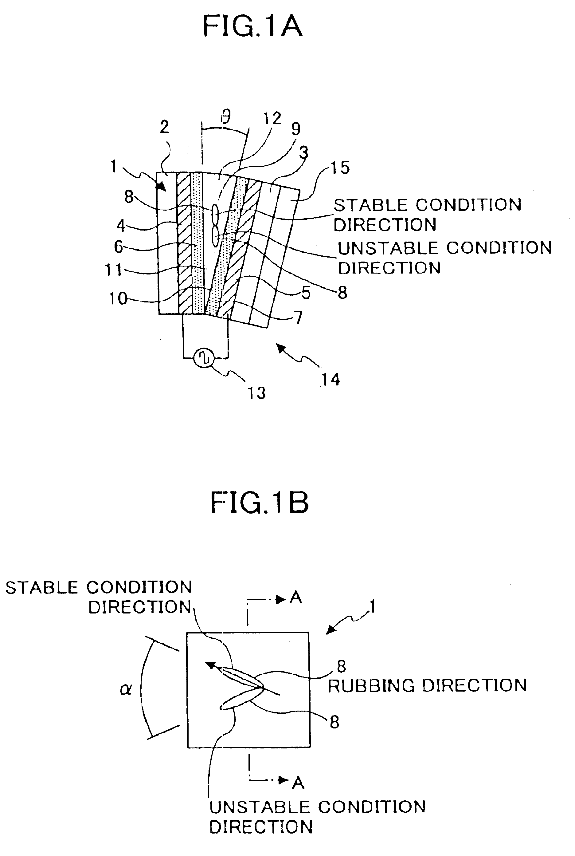
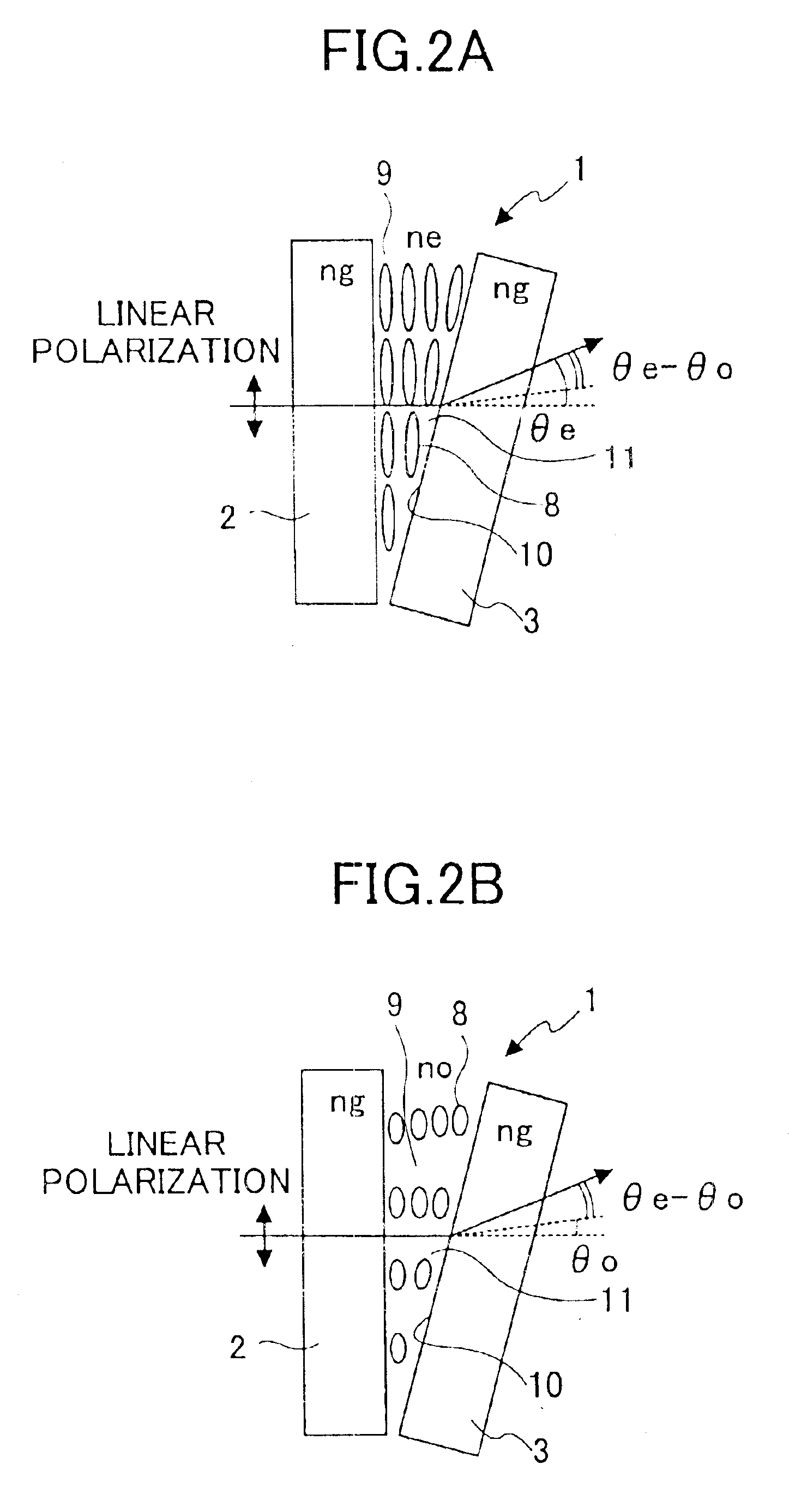
[0158]A description will now be given, with reference to FIG. 1 through FIG. 5, of an optical deflecting element according to the present invention. The optical deflecting element fundamentally changes a light exit angle on a slope surface through variations of a refractive index of liquid crystal molecules toward incident light by electrically alternating the alignment direction of the liquid crystal molecules. In this specification, the optical deflecting element means an optical element that can deflect an optical path in accordance with an external electronic signal, that is, an optical element that can shift incident light in parallel (parallel shift), rotate the incident light by a predetermined angle (angle deflection) or shift the optical path in a combination of the parallel shift and the angle deflection.

[0159]FIGS. 1A and 1B roughly show a structure of an optical deflecting element (optical element) and an optical deflecting apparatus according to the first embodiment. In...

fourth embodiment

[0198]A description will now be given, with reference to FIG. 11 and FIG. 12, of an optical path deflecting element 41 according to the present invention wherein the same parts as those in the previous embodiments are designated by the same reference numerals and the description thereof is omitted.

[0199]The optical path deflecting element 41 is constituted so that incident light can be shifted in parallel. FIG. 11 is a sectional view of the optical path deflecting element 41. As shown in FIG. 11, in the optical path deflecting element 41, the slope region 11 is divided between the substrates 2 and 3 into a first slope region 42 and a second slope region 43, and a transparent middle substrate 44 is provided so that the substrates 2 and 3 can be arranged at a predetermined space. The first and the second slope regions 42 and 43 have a first slope surface 45 and a second slope surface46, respectively, in the sides of the middle substrate 44. The first and the second slope surfaces 45 a...

fifth embodiment

[0203]A description will now be given, with reference to FIG. 13 and FIG. 14, of an optical path deflecting apparatus according to the present invention wherein the same parts as those in the previous embodiment are designated by the same reference numerals and the description thereof is omitted. When only one optical path deflecting element is used in an optical path deflecting apparatus as the above-mentioned embodiments, the optical path deflecting apparatus can deflect an optical path in just one direction. In an optical path deflecting apparatus according to this embodiment, two optical path deflecting elements 61 and 62 are combined. The combined optical path deflecting elements 61 and 62 are mounted to an optical path deflecting apparatus 63. At this time, the optical path deflecting apparatus 63 can deflect (shift) an optical path in two directions orthogonal to each other.

[0204]In the optical path deflecting apparatus 63, a first optical path deflecting element 61 and a sec...


PUM


Abstract

An optical path deflecting element, an optical path deflecting apparatus, an image displaying apparatus, an optical writing apparatus, an optical interconnection apparatus, an optical element, and a fabrication method thereof. The optical path deflecting element includes a pair of transparent substrates, transparent electrode films on the substrates to which a voltage having an inverse polarity is selectively applied, an alignment layer in the inner sides of the substrates, and a liquid crystal layer formed of a chiral smectic C phase between the substrates via the alignment layer and homogeneously aligned by the alignment layer. The optical deflecting element can realize the uniformly-aligned liquid crystal layer more easily than a case in which the liquid crystal is aligned to become in a bistable condition. For this reason, it is possible to improve yield in the fabrication.

Description

BACKGROUND OF THE INVENTION[0001]1. Field of the Invention[0002]The present invention generally relates to an optical path deflecting element, an optical path deflecting apparatus, an image displaying apparatus, an optical element, and a manufacturing method thereof.[0003]2. Description of the Related Art[0004]Conventionally, various optical elements are used as optical path deflecting elements. Among them, electrooptic devices formed of materials that have large primary electrooptic effect (Pockels effect), for instance, KH2PO4(KDP), NH4H2PO4(ADP), LiNbO3, LiTaO3, GaAs, CdTe, are well-known. Also, electrooptic devices formed of materials that have large secondary electrooptic effect, for instance, KTN, SrTiO3, CS2, nitrobenzene; are well-known. Furthermore, acoustic optical devices formed of materials, for instance, glass, silica, TeO2, are well-known (ref. “Optoelectronic Devices,” edited by S. Aoki, Shokodo). In these conventional optical elements, it is generally necessary to pr...

Claims


Application Information

Patent Timeline
IPC IPC(8): G02F1/13G02F1/1333G02F1/29G02F1/137G02F1/133G02F1/141G02F1/1335G02F1/13357G02F1/1337G02F1/1347
CPCG02F1/133371G02F1/29G02F1/13781
Inventor NIMURA, SHIGEAKIKOBAYASHI, MASANORISUGIMOTO, HIROYUKITAKIGUCHI, YASUYUKITOKITA, TOSHIAKIMATSUKI, YUMI
Owner RICOH KK
Why Eureka
Try Eureka