
Smart memory

a technology of integrated circuits and memory chips, applied in the field of smart memory, can solve the problems of increasing power consumption, reducing the active operation time of a mobile phone, and using a lot of more powerful processors at high data rates, and achieve the effect of increasing power consumption

Inactive Publication Date: 2005-07-19
NANOAMP SOLUTIONS
View PDF5 Cites 15 Cited by
  • Summary
  • Abstract
  • Description
  • Claims
  • Application Information

AI Technical Summary

Benefits of technology

[0021]It is therefore an object of the invention to provide a technique that adds additional functions for mobile communication and consumer electronics into a wireless appliance, such as a cell phone. The technique does not significantly increase power consumption and provides additional functions while keeping substantially the same fit and form as a standard integrated-circuit memory.
[0022]The present invention provides a smart memory device that includes a memory array and that incorporates one or more memory-intensive additional functions. All of these are packaged in a standard memory package to relieve the workload on a baseband chip. By incorporating these additional memory-intensive functions with a standard memory package such as, for example, a Flash-SRAM combination package, a number of advantages are obtained. These advantages include: elimination of the need for additional special function integrated-circuit packages; significant reduction of functions preformed by the baseband chip, and reduction of the clock rate and the power consumption of the baseband chip.

Problems solved by technology

Running more powerful processors at high data rates uses a lot of power, which can rapidly drain a battery and thereby reduce the active operation time of a mobile handset.
This further increases power consumption and drains the battery.
Additional integrated circuits increase the size of a printed circuit in the cell-phone, increase the cell-phone weight, require more inventory and control of the additional integrated circuits, and add additional cost for the additional integrated circuits.
However, it should also be appreciated that the cell-phone industry trend toward adding more functions to a single baseband integrated circuit or to a baseband chip set increases the complexity of the base-band integrated circuit or chip set and requires additional signal processing power in the baseband integrated circuit.
For example, the basic microcontroller unit used in the baseband chips has changed from an ARM 7 to 9 to an ARM 10 to 11, while the clock cycle rate has gone from tens of megahertz to a few hundred Megahertz These large increases in performance requirements for a single baseband integrated circuit or a baseband chip set have increased the size, number, complexity, and cost of baseband integrated circuits.
This will significantly increase the power consumption of the baseband integrated circuit and will rapidly drain a cell-phone battery, reducing the usable time between cell-phone battery charges.
Consequently, a need exists for a technique that adds additional memory-intensive functions into portable electronic devices, such as a wireless appliance or a cell phone, but that does not increase package count and power consumption while keeping substantially the same fit and form as a standard memory integrated circuit.

Method used


Image

  • Smart memory
  • Smart memory
  • Smart memory

Examples


Embodiment Construction

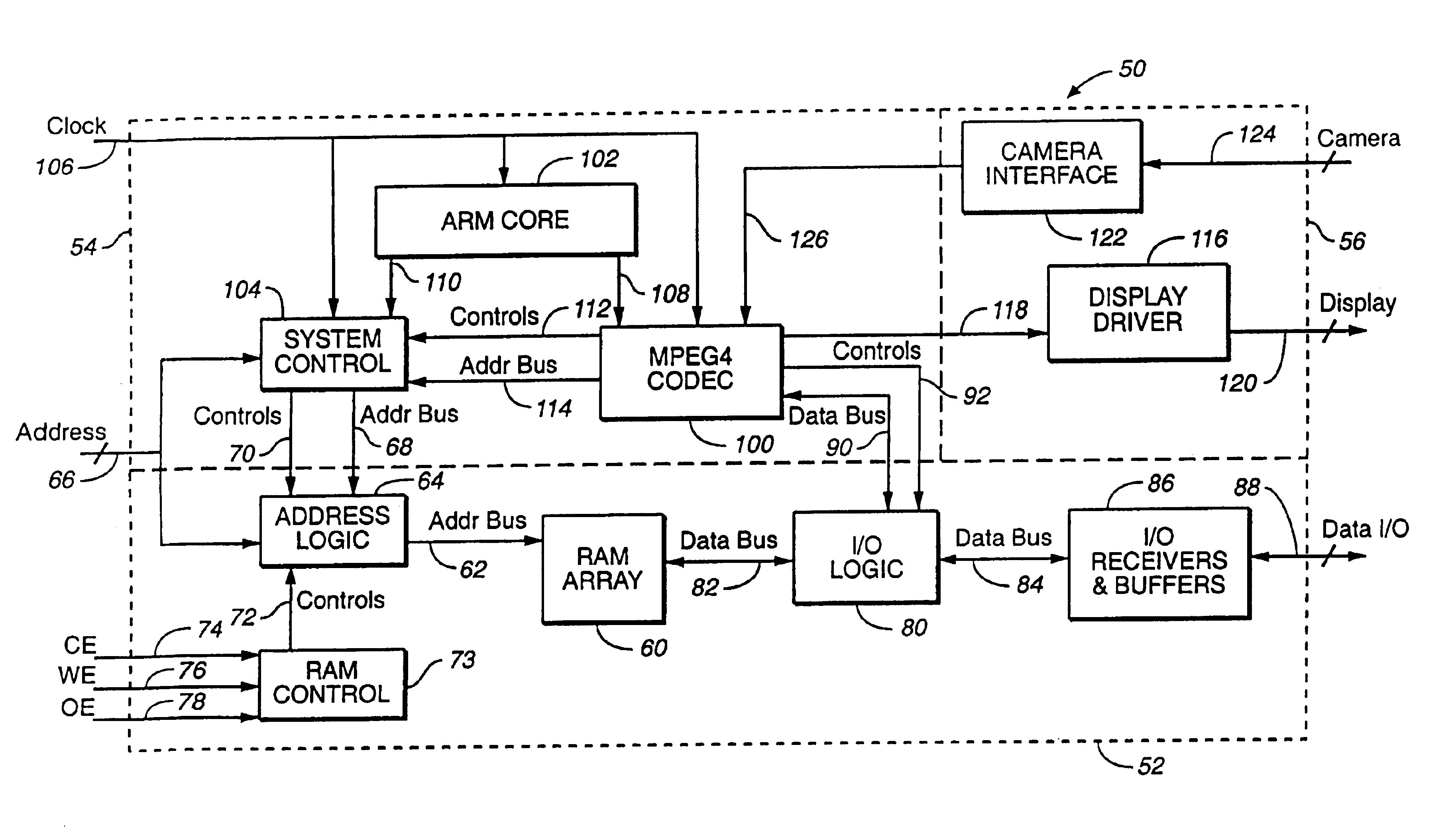
[0042]Reference is now made in detail to preferred embodiments of the invention, examples of which are illustrated in the accompanying drawings. While the invention is described in conjunction with these preferred embodiments, it will be understood that it is not intended to limit the invention to these embodiments. On the contrary, the invention is intended to cover alternatives, modifications and equivalents, which may be included within the spirit and scope of the invention as defined by the appended claims.

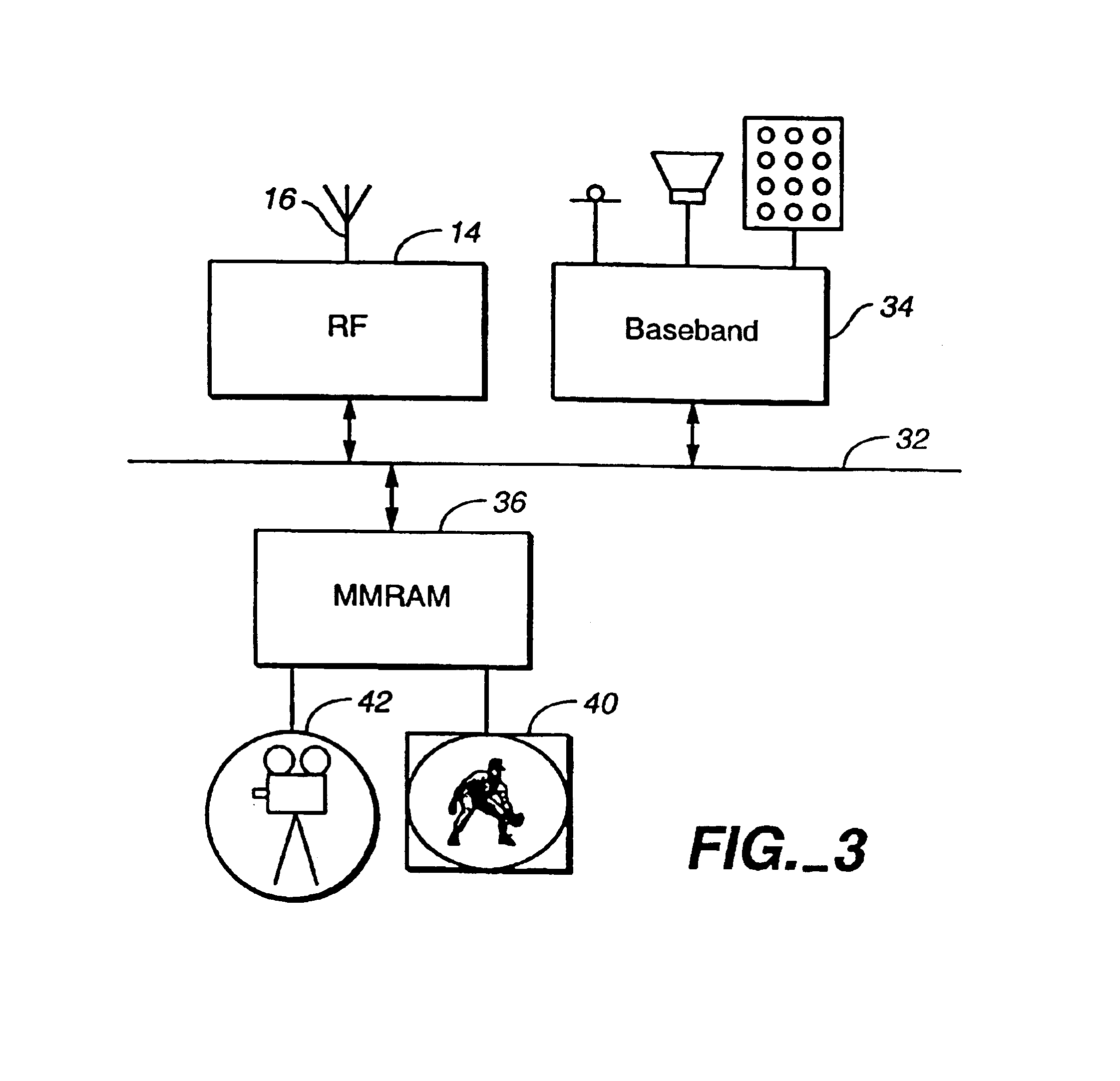
[0043]FIG. 3 shows a general system architecture according to the present invention for implementing a multimedia wireless system 30 that is used in a typical wireless communication device, such as a cell phone handset. In contrast to the conventional system of FIG. 2, the wireless communication system 30 includes integrated-circuit packages that communicate much less with each other through a system printed-circuit bus 32. There are some significant differences between the co...


PUM


Abstract

A smart memory includes a memory array and one or more memory-intensive additional functions, all packaged in a standard memory package that has substantially the same fit and form as a standard integrated-circuit memory. One type of smart memory chip is a multi-media RAM (MMRAM) chip that provides on a single integrated-circuit chip a memory array and a compressor / decompressor (CODEC) section where connections between the memory array section and the CODEC section are on the single integrated-circuit die. The smart memory eliminates the need for additional special function integrated-circuit packages and significantly reduces the clock rate and the power consumption of a baseband chip in a personal communication device.

Description

[0001]This is a continuation of U.S. patent application Ser. No. 09 / 898,520 that was filed Jul. 2, 2001, now U.S. Pat. No. 6,681,287 and that is incorporated by reference herein.BACKGROUND OF THE INVENTION[0002]1. Field of the Invention[0003]The present invention relates to integrated-circuit (IC) memory chips and, more particularly, to an enhanced integrated circuit memory chips that incorporate additional functions in a standard memory package.[0004]2. Prior Art[0005]Portable electronic devices such as laptop computers, cell phones, personnel digital assistants (PDA's), handheld or portable game consoles from companies such as Nintendo, Sony, and other portable electronic devices, all use standard integrated-circuit memories. Standard memories include, but are not limited to: static random access memory (SRAM), pseudo-SRAM, dynamic random access memory (DRAM), Flash memory, electronically erasable programmed read only memory (EEPROM), electronically programmed read only memory (EP...

Claims


Application Information

Patent Timeline
IPC IPC(8): G11C7/10G06K19/07
CPCG11C7/1006
Inventor CHAN, HUGO W. K
Owner NANOAMP SOLUTIONS
Learn More