Power MOSFET and method for forming same using a self-aligned body implant

a self-aligning body and implant technology, applied in the field of semi-conductor devices, can solve the problems of poor soa, reduced ruggedness of devices, and reduced ruggedness of devices, and achieve the effects of reducing on-resistance, increasing device ruggedness, and reducing on-resistan

Inactive Publication Date: 2005-07-26
SEMICON COMPONENTS IND LLC
View PDF44 Cites 31 Cited by
  • Summary
  • Abstract
  • Description
  • Claims
  • Application Information

AI Technical Summary

Benefits of technology

[0010]It is another object of the present invention to provide the trench-gated power MOSFET without decreasing device ruggedness.
[0013]The resulting trench-gated power MOSFET is advantageously formed with a reduced on-resistance without degrading device ruggedness. The on-resistance is reduced since each MOSFET includes a source / body contact region. The source / body contact region provides an efficient short between the source and body regions of the MOSFET. As a result, device ruggedness is increased.
[0014]In addition, the on-resistance is reduced because the cell pitch of the power MOSFET is reduced as a result of the dielectric layer being formed completely within the trench. In other words, the dielectric layer is not on the surface of the source regions which would minimize the contact region between the source regions and the source electrode.
[0015]Another factor for reducing the on-resistance and the cell pitch of the power MOSFET is a result of using the spacers as a self-aligned mask for implanting dopants into the body region for defining the source / body contact regions. Since the spacers are self-aligned with the outwardly extending dielectric layer, source / body contact masking misalignment tolerances are avoided.
[0016]Another embodiment of the present invention is to further use the spacers as a self-aligned mask for removing a portion of the semiconductor layer not covered by the spacers prior to defining the source / body contact regions. With a portion of the semiconductor layer removed, lower energy is needed to implant the dopants for forming the source / body contact regions.
[0017]In addition, the source / body contact regions can preferably be formed deeper within the semiconductor layer as a result of a portion thereof being removed. This decreases the base resistance and the common base current gain of the parasitic BJT, which improves device ruggedness, i.e., the safe operating range (SOA) and the unclamped inductive switching (UIS) of the power MOSFET are increased.

Problems solved by technology

But often this is accompanied by a decrease in device ruggedness.
Unfortunately, the periodic placement of the P+ source / body contact region 18 increases the on-resistance of the device 28, as well as the base resistance and the common base current gain of the parasitic BJT.
As a consequence, the parasitic BJT will be turned on at a very low current, resulting in a poor SOA and a lower UIS capability.

Method used


Image

  • Power MOSFET and method for forming same using a self-aligned body implant
  • Power MOSFET and method for forming same using a self-aligned body implant
  • Power MOSFET and method for forming same using a self-aligned body implant

Examples


Embodiment Construction

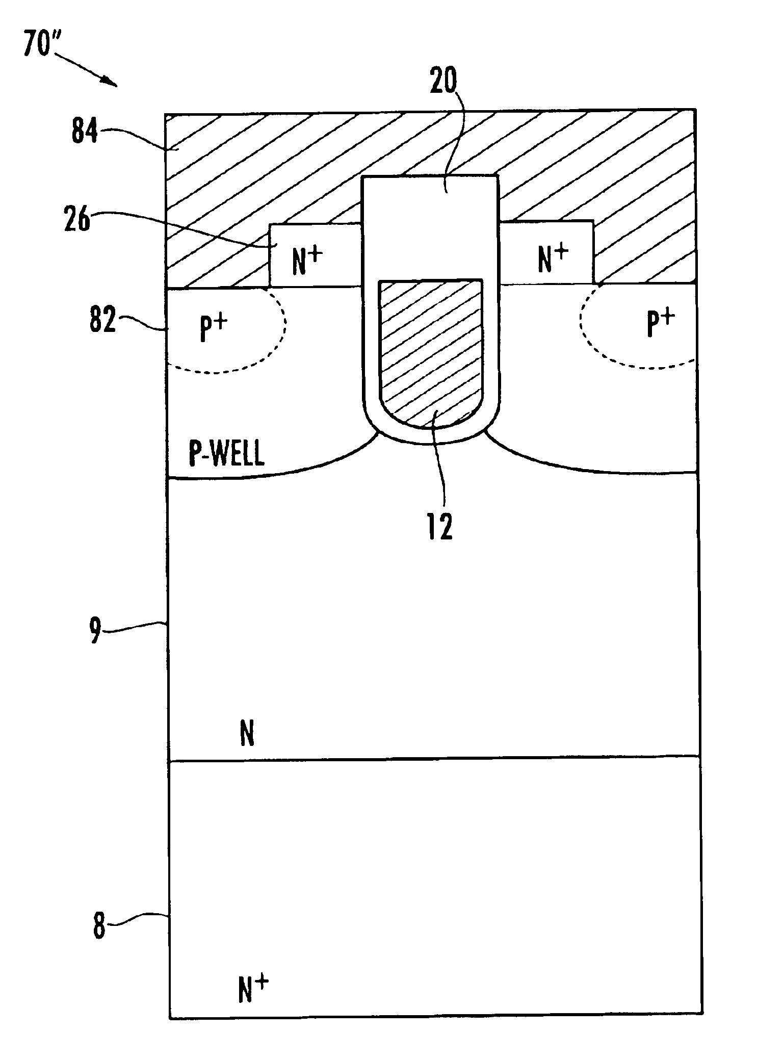
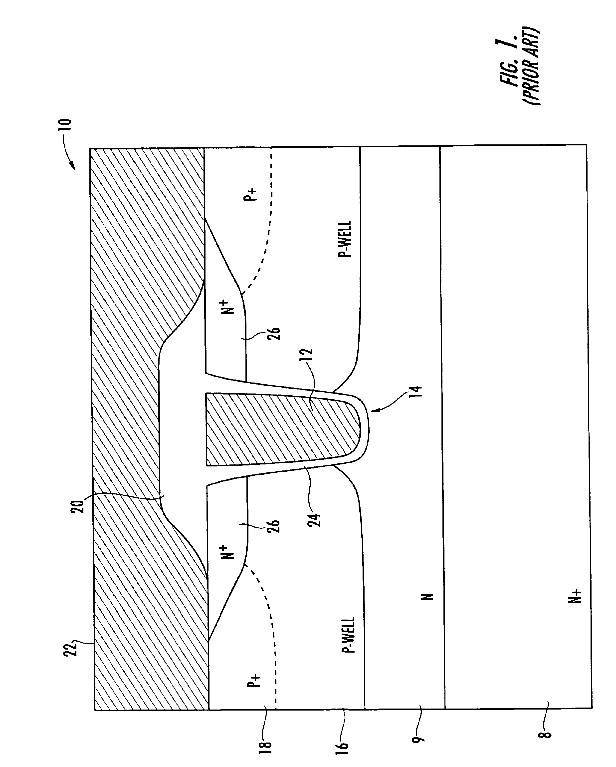
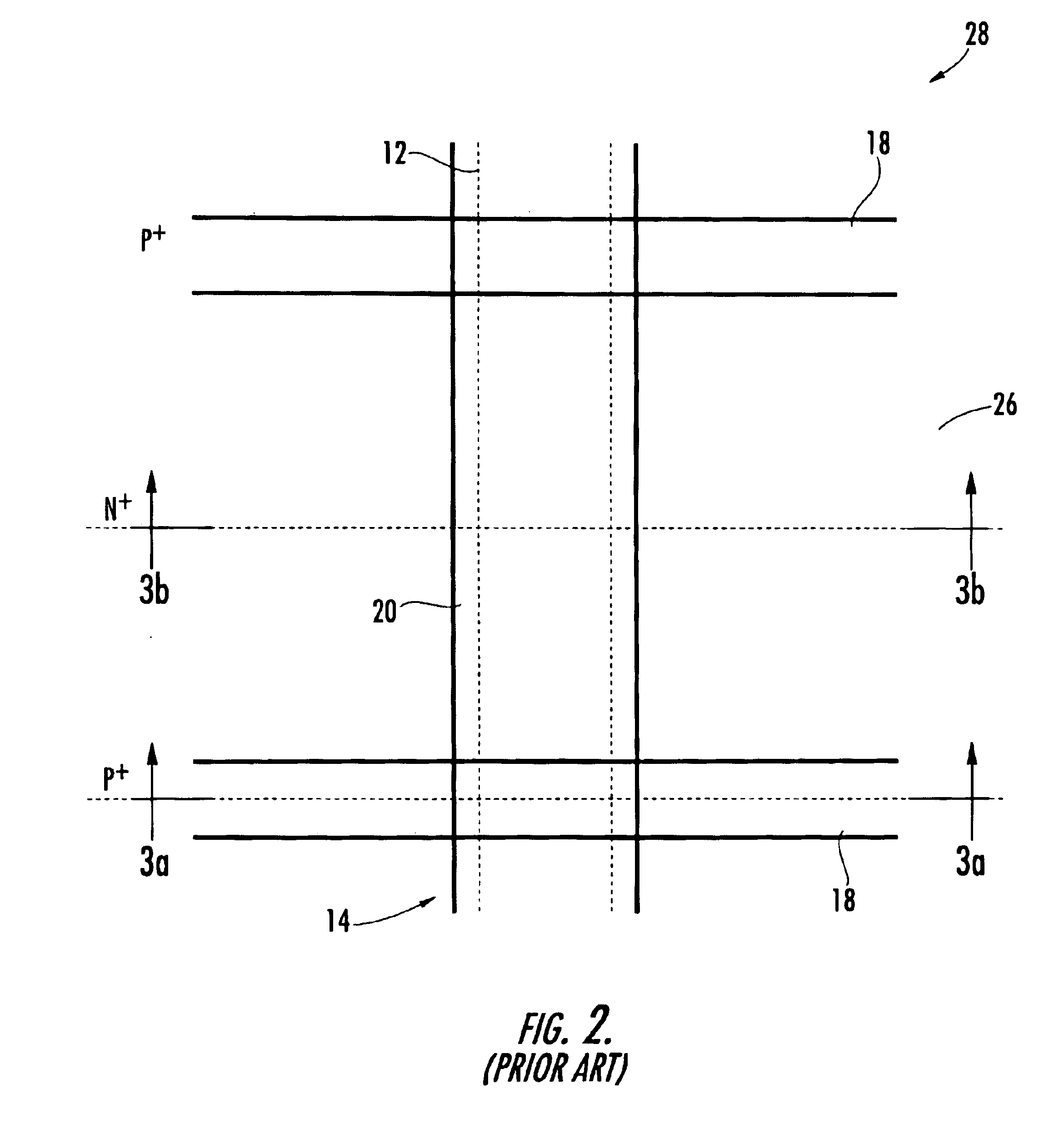
[0028]The present invention will now be described more fully hereinafter with reference to the accompanying drawings, in which preferred embodiments of the invention are shown. This invention may, however, be embodied in many different forms and should not be construed as limited to the embodiments set forth herein. Rather, these embodiments are provided so that this disclosure will be thorough and complete, and will fully convey the scope of the invention to those skilled in the art. Like numbers refer to like elements throughout. The dimensions of layers and regions may be exaggerated in the figures for greater clarity.

[0029]Referring now to FIG. 4, a method for making a trench-gated power MOSFET in accordance with the present invention is described. From the start (Block 40), a trench is formed in a semiconductor layer at Block 42, and a gate dielectric layer is formed to line the trench at Block 44. A gate conducting layer is then formed in a lower portion of the trench at Block...


PUM


Abstract

A method for making a power MOSFET includes forming a trench in a semiconductor layer, forming a gate dielectric layer lining the trench, forming a gate conducting layer in a lower portion of the trench, and forming a dielectric layer to fill an upper portion of the trench. Portions of the semiconductor layer laterally adjacent the dielectric layer are removed so that an upper portion thereof extends outwardly from the semiconductor layer. Spacers are formed laterally adjacent the outwardly extending upper portion of the dielectric layer, the spacers are used as a self-aligned mask for defining source / body contact regions.

Description

RELATED APPLICATION[0001]This application is based upon prior filed copending provisional application No. 60 / 219,858 filed Jul. 20, 2000, the entire disclosure of which is incorporated herein by reference.FIELD OF THE INVENTION[0002]The present invention relates to the field of semiconductor devices, and, more particularly, to a trench-gated power MOSFET.BACKGROUND OF THE INVENTION[0003]The electronic industry has demonstrated a great need for small discrete power MOSFETs with low on-resistances (RDSon), large blocking voltages (VDSBR), and low gate charges in addition to adequate ruggedness. Ruggedness defines the safe operating area (SOA) and the unclamped inductive switching (UIS) of the device. With an optimum combination of these characteristics, extremely low on-state power losses and switching losses can be achieved, resulting in high power conversion efficiencies in systems such as DC-DC converters.[0004]Ultra dense trench-gated power MOSFET technology has been developed to ...

Claims


Application Information

Patent Timeline
IPC IPC(8): H01L21/336H01L29/78H01L21/02H01L29/10H01L29/02H01L29/66H01L29/417H01L29/423H01L29/40
CPCH01L29/1095H01L29/7813H01L29/41741H01L29/41766H01L29/4232H01L29/4238H01L29/7802Y10S257/905H01L2924/0002H01L2924/00H01L29/66734H01L29/66727
Inventor ZENG, JUN
Owner SEMICON COMPONENTS IND LLC
Why Eureka
Try Eureka