High speed sampling receiver with reduced output impedance

a high-speed sampling and output impedance technology, applied in the field of sampling receivers, can solve the problems of increasing the delay time of latches, and the apparent driving ability of transistors, so as to reduce the delay time, increase the common mode level of input signals, and high-speed latch operation

Inactive Publication Date: 2005-07-26
RENESAS ELECTRONICS CORP
View PDF13 Cites 15 Cited by
  • Summary
  • Abstract
  • Description
  • Claims
  • Application Information

AI Technical Summary

Benefits of technology

[0029]It is still more object of the present invention to provide a novel high speed sampling receiver exhibiting a high speed latch operation and allowing an enlarged common mode level of input signals.
[0030]It is another object of the present invention to provide a novel master latch circuit allowing a high speed sampling receiver to be free from the above problems.
[0031]It is further another object of the present invention to provide a novel master latch circuit allowing a high speed sampling receiver to reduce a delay time in falling an output signal from a master latch circuit.
[0032]It is still furthe...

Problems solved by technology

The relatively large time constant of the falling output signal makes the transistor driving ability small apparently.
Namely, the relatively large time constant of the falling output signal increases a delay time in falling of the output signal from the master latch circuit.
The increase in the delay ti...

Method used


Image

  • High speed sampling receiver with reduced output impedance
  • High speed sampling receiver with reduced output impedance
  • High speed sampling receiver with reduced output impedance

Examples


first embodiment

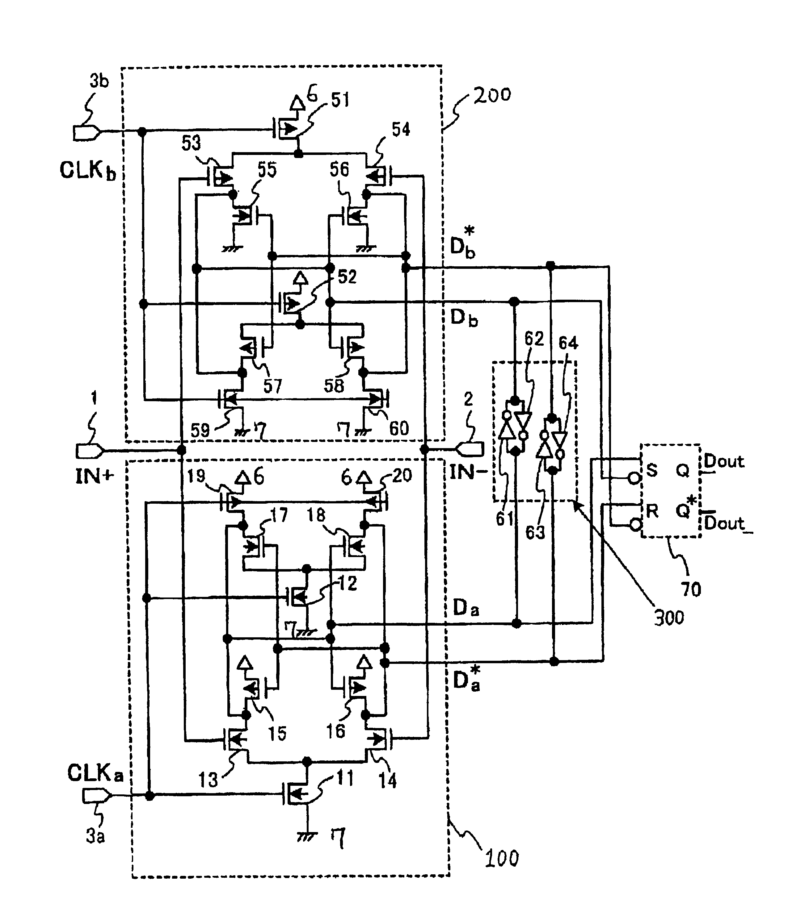
[0061]A first embodiment according to the present invention will be described in detail with reference to the drawings. FIG. 3 is a circuit diagram illustrative of a circuit configuration of one typical novel sampling receiver in a first embodiment in accordance with the present invention. The sampling receiver has the following circuit configuration.

[0062]The sampling receiver includes a master latch circuit and a slave latch circuit. The slave latch circuit comprises a set-reset-flip-flop circuit 50 which has two input terminals “S” and “R” and two output terminals 4“Q” and 5“Q*”. The input terminal “S” of the slave latch circuit receives the output “D” from the master latch circuit. The input terminal “R” of the slave latch circuit receives the output “D*” from the master latch circuit.

[0063]The master latch circuit includes a differential input transistor pair and a bistable circuit. The bistable circuit comprises two CMOS inverters. The differential input transistor pair furthe...

second embodiment

[0082]A second embodiment according to the present invention will be described in detail with reference to the drawings. FIG. 5 is a circuit diagram illustrative of a circuit configuration of one typical novel sampling receiver in a second embodiment in accordance with the present invention. The sampling receiver of this second embodiment has the following circuit configuration which is different from the first embodiment in including both a first differential input transistor pair of two n-channel MOS field effect transistors 13 and 14 and a second differential input transistor pair of two p-channel MOS field effect transistors 23 and 24.

[0083]The sampling receiver includes a master latch circuit and a slave latch circuit. The slave latch circuit comprises a set-reset-flip-flop circuit 50 which has two input terminals “S” and “R” and two output terminals 4“Q” and 5“Q*”. The input terminal “S” of the slave latch circuit receives the output “D” from the master latch circuit. The inpu...

third embodiment

[0100]A third embodiment according to the present invention will be described in detail with reference to the drawings. FIG. 7 is a circuit diagram illustrative of a circuit configuration of one typical novel sampling receiver in a third embodiment in accordance with the present invention. The sampling receiver of this third embodiment has the following circuit configuration which is different from the second embodiment in the absence of the current-supplying p-channel MOS field effect transistor 25 and the series connection of the two inverters 26 and 27.

[0101]The sampling receiver includes a master latch circuit and a slave latch circuit. The slave latch circuit comprises a set-reset-flip-flop circuit 50 which has two input terminals “S” and “R” and two output terminals 4“Q” and 5“Q*”. The input terminal “S” of the slave latch circuit receives the output “D” from the master latch circuit. The input terminal “R” of the slave latch circuit receives the output “D*” from the master la...


PUM


Abstract

A sampling receiver includes: at least one slave latch circuit; and at least one master latch circuit which further includes: at least one differential input transistor pair, and at least one bistable circuit. Output terminals of the at least one differential input transistor pair and output terminals of the at least one bistable circuit are coupled to the at least one slave latch circuit but in parallel to each other with reference to the at least one slave latch circuit for the purpose of reducing an output impedance to allow the sampling receiver to exhibit a high speed latch operation.

Description

BACKGROUND OF THE INVENTION[0001]1. Field of the Invention[0002]The present invention relates to a sampling receiver, and more particularly to a high speed sampling receiver for sampling data with a small amplitude and latching the same to convert a voltage level of the latched data into an adjusted voltage level to a CMOS circuit.[0003]All of patents, patent applications, patent publications, scientific articles and the like, which will hereinafter be cited or identified in the present application, will, hereby, be incorporated by references in their entirety in order to describe more fully the state of the art, to which the present invention pertains.[0004]2. Description of the Related Art[0005]Data which have been read out from semiconductor memory devices such as DRAM may have a relatively small amplitude, while data to be inputted into the CMOS circuit should have a relatively high amplitude or a high voltage level. A sampling receiver has been used for sampling the small ampli...

Claims


Application Information

Patent Timeline
IPC IPC(8): H03K3/3562H03K3/356H03K3/00H03K3/012H03K17/00H03K3/0233H03K19/0185
CPCH03K3/356139H03K3/35625H03K3/012H03K3/0233
Inventor TANAKA, KENICHIMINAMI, KOUICHIROU
Owner RENESAS ELECTRONICS CORP
Why Eureka
Try Eureka