System and method for achieving timing closure in fixed placed designs after implementing logic changes
- Summary
- Abstract
- Description
- Claims
- Application Information
AI Technical Summary
Benefits of technology
Problems solved by technology
Method used
Image

Examples
Embodiment Construction
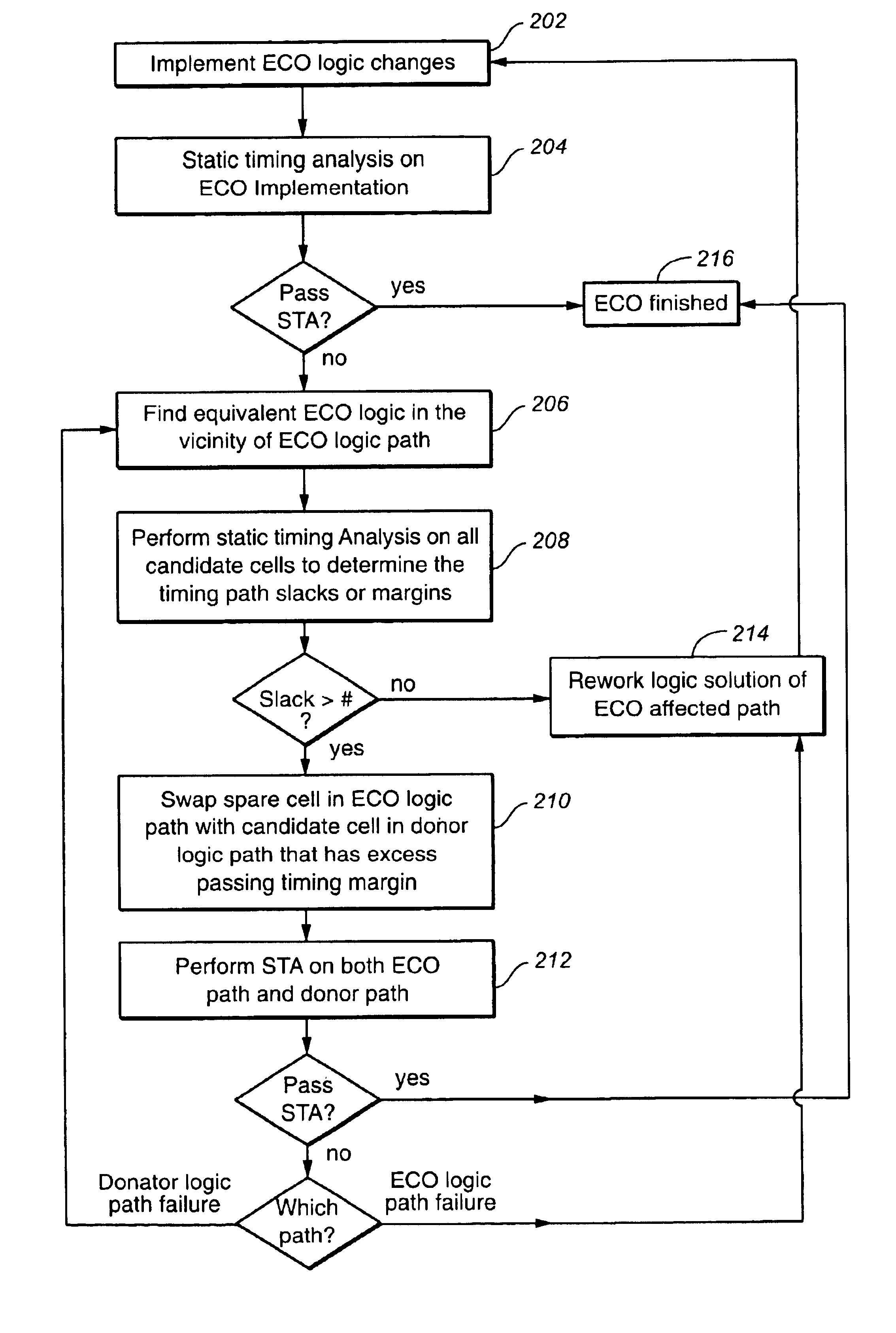
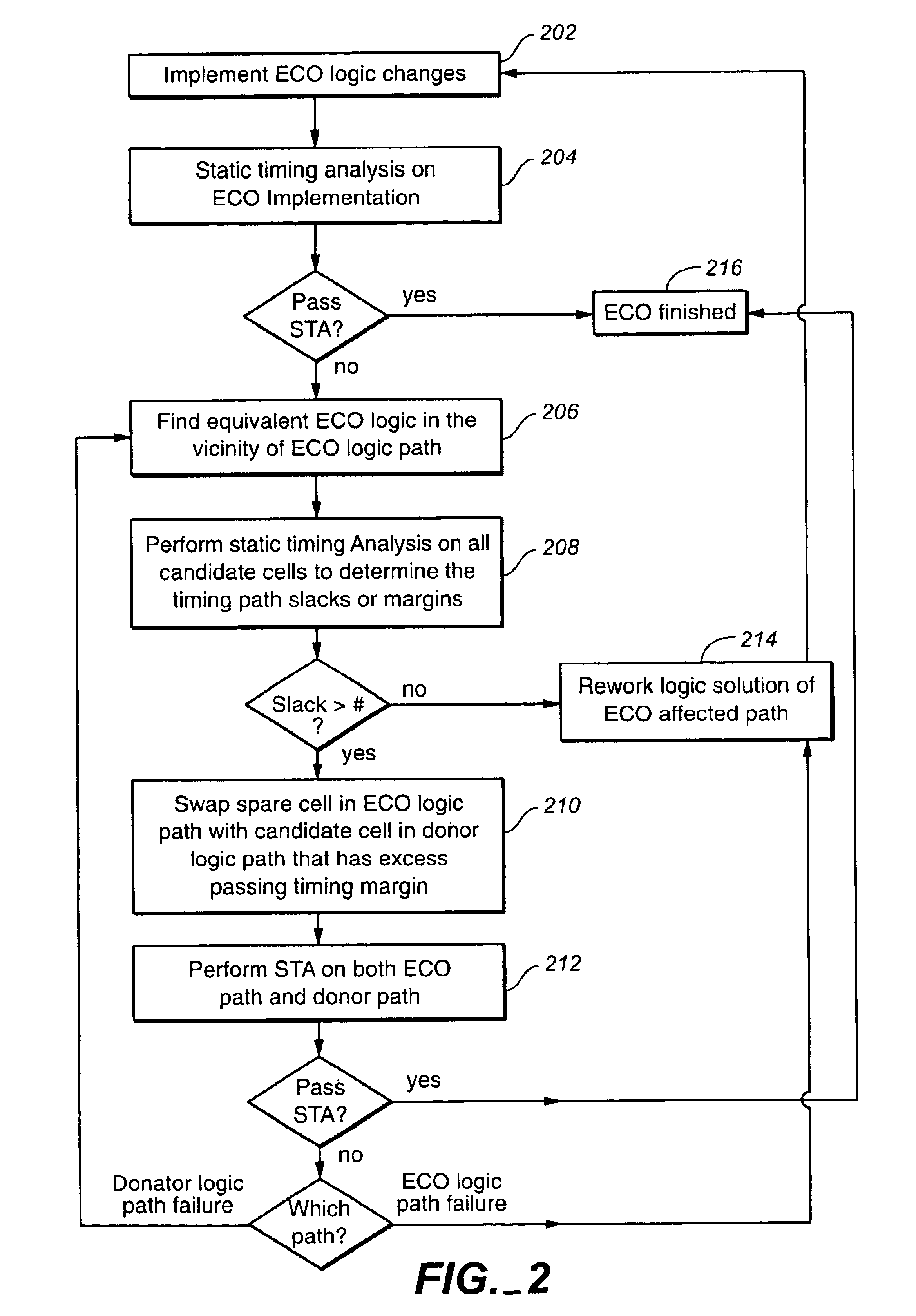
[0015]The present invention is described with reference to the Figures.
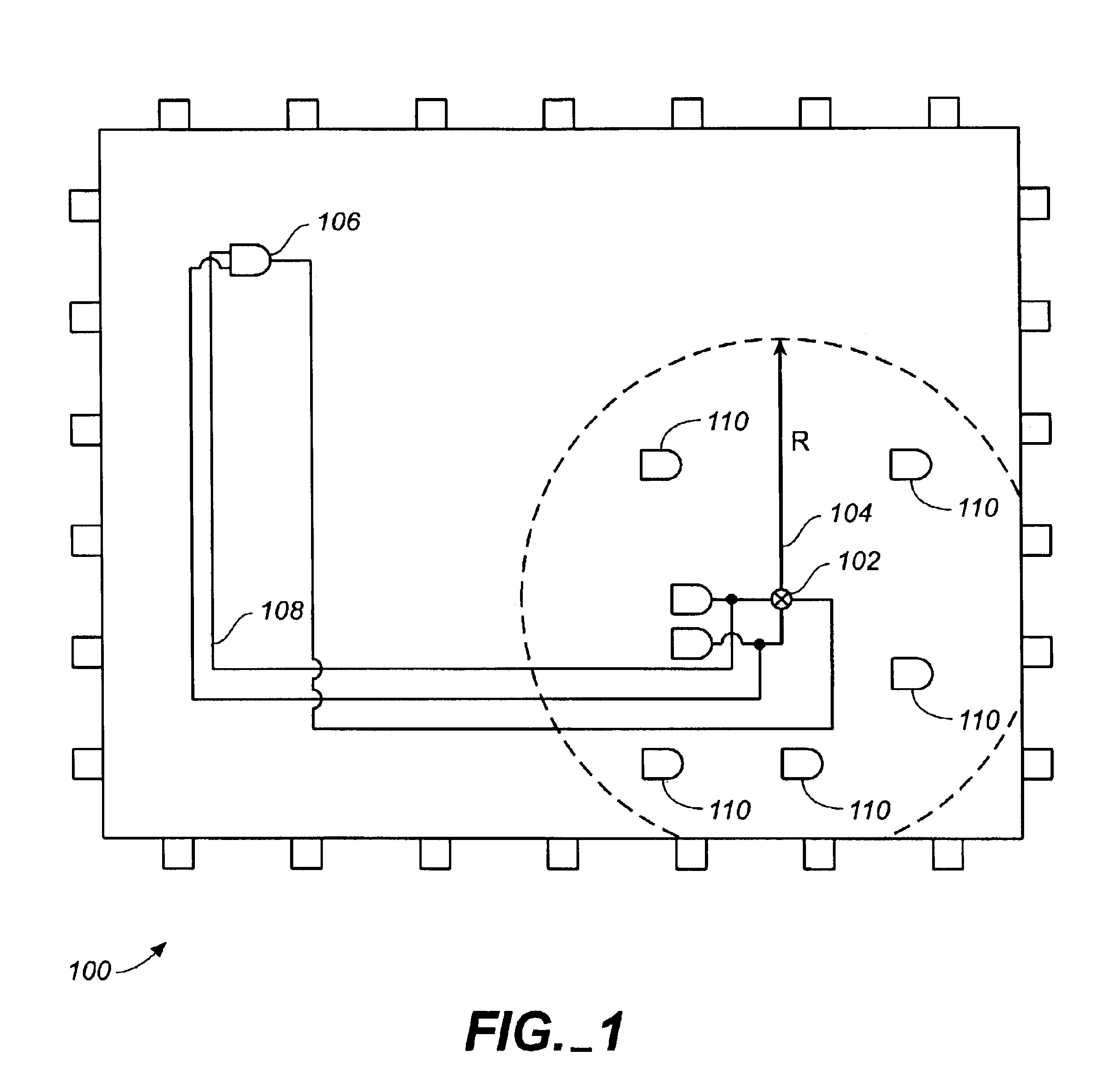
[0016]FIG. 1 shows a an example of an integrated circuit chip in which the present invention can be implemented. This diagram shows a top view of an IC chip 100. In this example, an ECO design adds a logic element to an existing logic path. The preferred location 102 of this added logic element is shown by an “X”. The diagram shows a radius R 104 centered on the preferred location 102. Radius 104 can vary depending on the timing margins associated with the various paths. If timing margins are generally narrow, a smaller radius could be used to weed out candidates likely to end in timing closure failure. Example radii can be on the order of 200 microns, but depends ultimately on the exact implementation. Also shown is an extra or spare logic cell 106 that is located at a relatively large distance from the preferred location 102.
[0017]In this example embodiment, the ECO specifies an added logic element to an existi...
PUM
 Abstract
Description
Claims
Application Information
 - R&D Engineer
- R&D Manager
- IP Professional
- Industry Leading Data Capabilities
- Powerful AI technology
- Patent DNA Extraction
Browse by: Latest US Patents, China's latest patents, Technical Efficacy Thesaurus, Application Domain, Technology Topic.
© 2024 PatSnap. All rights reserved.Legal|Privacy policy|Modern Slavery Act Transparency Statement|Sitemap