Method for fabricating a bipolar transistor base

a bipolar transistor and base technology, applied in the direction of basic electric elements, electrical equipment, semiconductor devices, etc., can solve the problems of limited further reliably decreasing the base width of current methods for forming hbts

Inactive Publication Date: 2005-08-09
INTEL CORP
View PDF10 Cites 28 Cited by
  • Summary
  • Abstract
  • Description
  • Claims
  • Application Information

AI Technical Summary

Problems solved by technology

HBTs are used in these devices because of their high cut off frequencies greater than 150 gigahertz (Ghz) even though they consume more power than equivalent metal oxide semiconductor (MOS) based technologies.
However, current methods for forming HBTs are limited in further reliably decreasing the base width because such methods are generally unable to create adequate boron concentration in a base region with reduced base width while controlling the SiGe deposition rate.

Method used


Image

  • Method for fabricating a bipolar transistor base
  • Method for fabricating a bipolar transistor base
  • Method for fabricating a bipolar transistor base

Examples


Embodiment Construction

[0020]Exemplary embodiments are described with reference to specific configurations and techniques. Those of ordinary skill in the art will appreciate the various changes and modifications to be made while remaining within the scope of the appended claims. Additionally, well known elements, devices, components, circuits, process steps and the like are not set forth in detail.

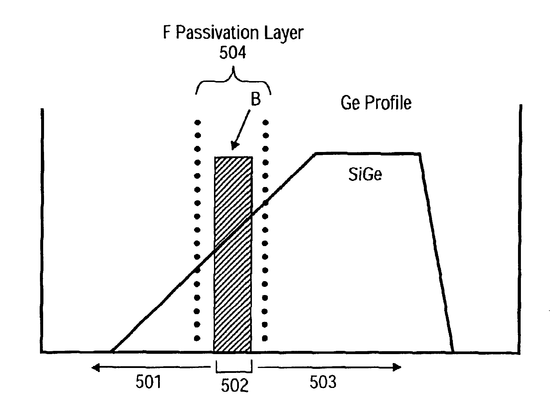
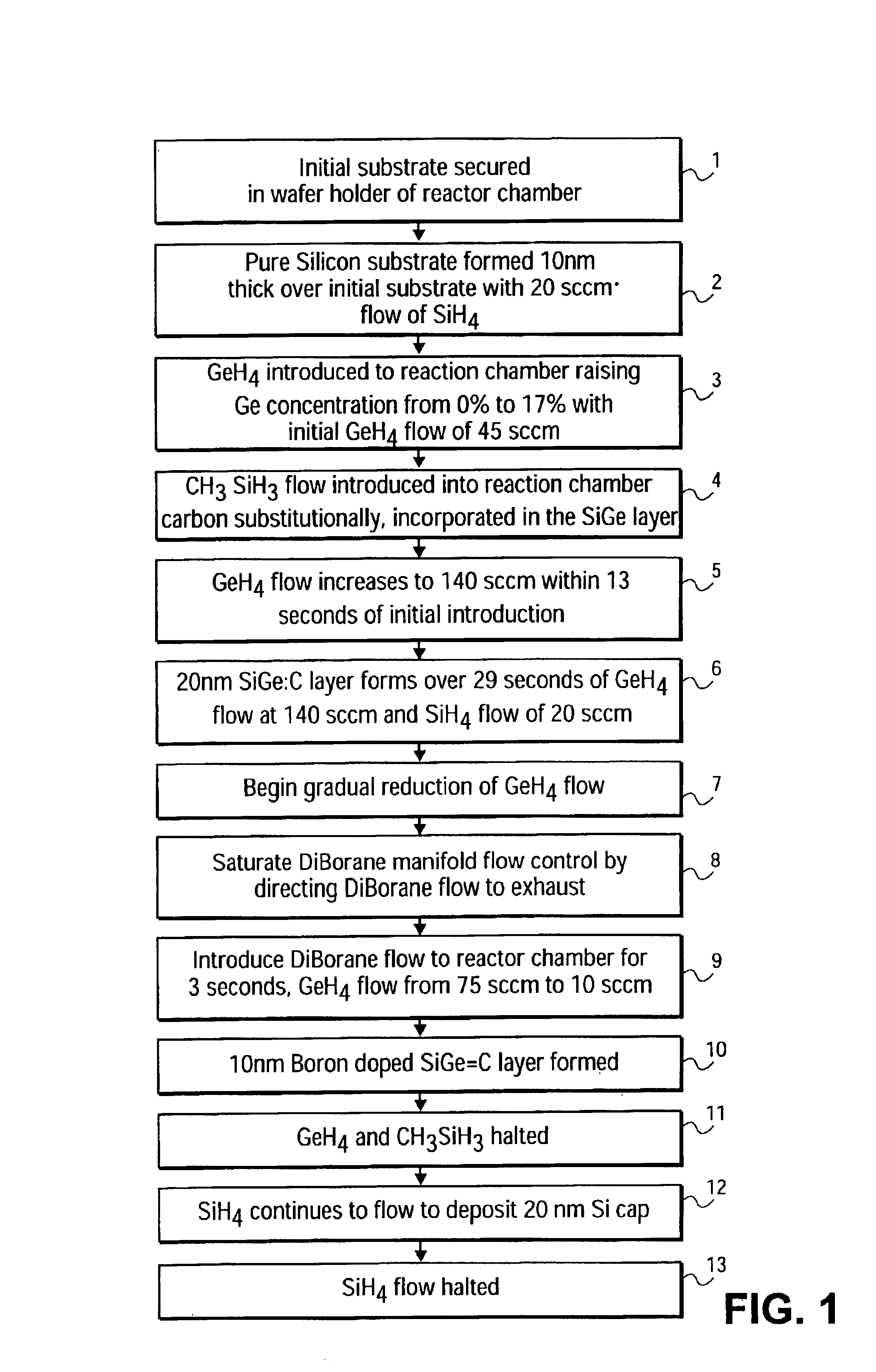
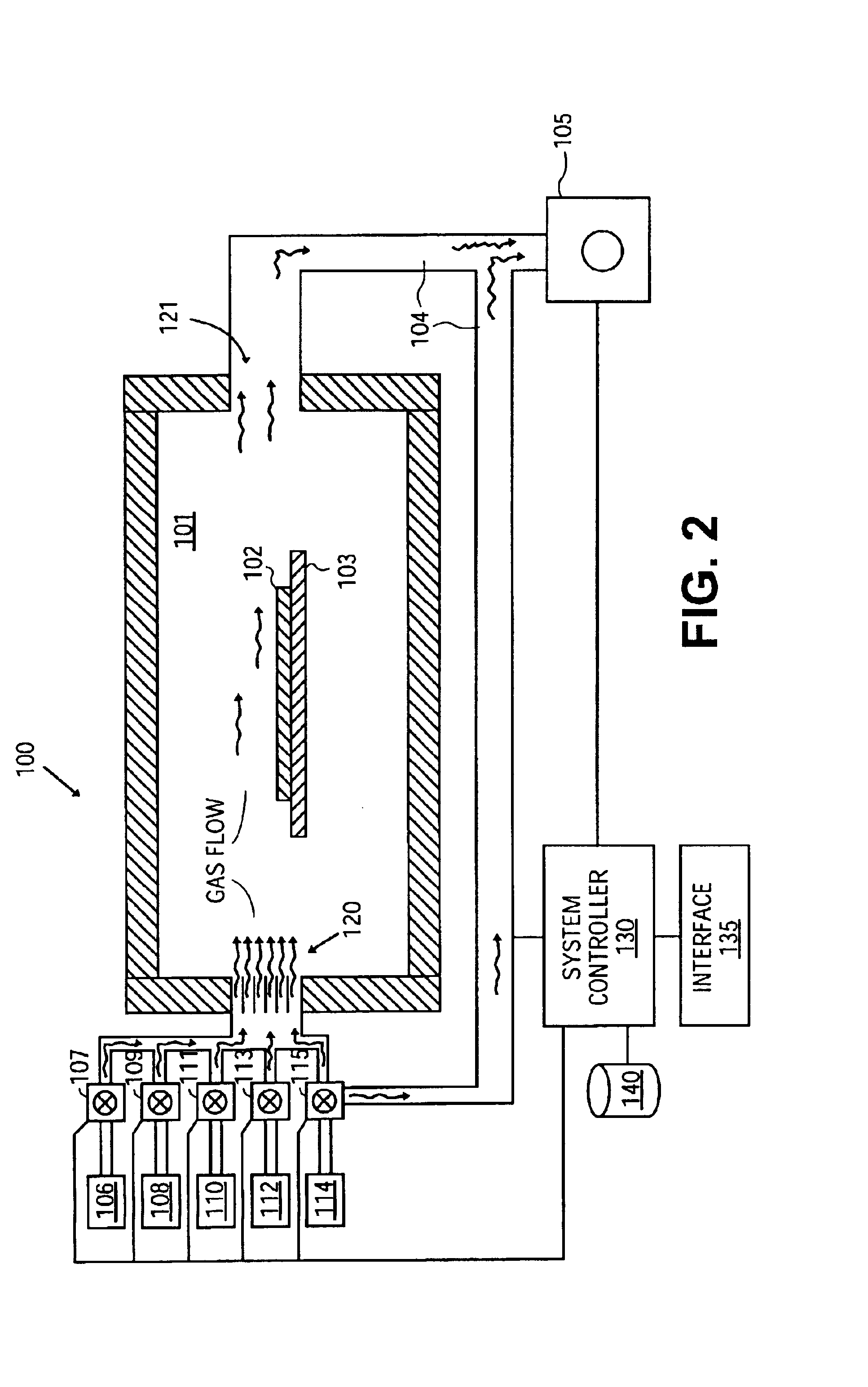
[0021]FIG. 1 is a flow chart of one embodiment of a method of forming a heterojunction bipolar transistor (HBT). FIG. 2 illustrates a substrate in a chamber undergoing the method described in FIG. 1. FIGS. 7-12 show the formation of an HBT on a substrate according to one method.

[0022]Referring to FIG. 1, a wafer or substrate is placed in a reactor (block 1). Referring to FIG. 2, Reactor 100 includes reactor chamber 101. In one embodiment, the chamber is that of an Epsilon® E3000 300 millimeters (mm) Epitaxial Reactor or E2500 or E2000 200 mm Epitaxial Reactor manufactured by ASM, Inc. Within reactor chamber 101 ...


PUM

PropertyMeasurementUnit
chamber pressureaaaaaaaaaa
temperatureaaaaaaaaaa
widthaaaaaaaaaa

Abstract

A method for forming a base of a bipolar transistor. A narrow base is formed using a flash of boron doping gas in a reaction chamber to create a narrow base with high boron concentration. This method allows for reliable formation of a base with high boron concentration while maintaining manageability in controlling deposition of other materials in a substrate.

Description

BACKGROUND[0001]1. Field[0002]Circuit fabrication, including a method for forming a base region of a bipolar transistor.[0003]2. Description of the Related Art[0004]Bipolar transistors, more specifically heterojunction bipolar transistors (HBTs) are used in devices requiring high frequency operation such as wireless and networking devices. HBTs are used in these devices because of their high cut off frequencies greater than 150 gigahertz (Ghz) even though they consume more power than equivalent metal oxide semiconductor (MOS) based technologies.[0005]HBTs typically consist of an emitter region, base region and collector region. The emitter region generally has a larger band gap than the base region to achieve high frequency performance. The speed at which the HBT can switch is referred to as the cutoff frequency, ft. The cutoff frequency of a given HBT is generally related to the width of its base region. The narrower the base region of a HBT, the shorter the base transit time and h...

Claims


Application Information

Patent Timeline
Patent Type & Authority Patents(United States)
IPC IPC(8): H01L21/331H01L29/10H01L21/205H01L29/02H01L21/02
CPCH01L21/02381H01L21/02532H01L21/02579H01L21/0262H01L29/1004H01L29/66242
Inventor SOMAN, RAVINDRAMURTHY, ANAND
Owner INTEL CORP
Why Eureka
Try Eureka