Contactor for testing miniaturized devices and components

Inactive Publication Date: 2005-08-09
SOCIONEXT INC
View PDF13 Cites 55 Cited by
  • Summary
  • Abstract
  • Description
  • Claims
  • Application Information

AI Technical Summary

Benefits of technology

[0050]Further, according to the contactor of the present invention, it becomes possible to prevent the deformation of the substrate even in the case there is a difference of coefficient of thermal expansion between the substrate and a spacer provided between adjacent substrates, as the substrate follows the thermal expansion of the spacer Further, according to the contactor of the present invention, it is possible to align the contact terminals accurately to t

Problems solved by technology

When the size of the chips is different, it should be noted that the compatibility of the handling equipment used for the testing is lost.
However, as noted before, it has been difficult to realize a conductor that can contact the terminals of plural LSIs on a wafer or the terminals of entire LSIs on the wafer, in view of miniaturization of individual LSIs and hence the terminals thereof, and further in view of increasing number of the terminals.
a) High cost of forming a large number of needles or pins individually;
b) Limitation in the precision of the needle tip due to the construction in which a large number of needles are arranged individually; and
c) Restriction imposed on the arrangement of the needles in view of the oblique arrangement of the needles.
Thus, it has been difficult to use a needle type mechanical probe for the contactor that makes a contact with plural LSIs at the same time.
Because the contact electrode is connected to a polyimide layer forming the insulating substrate, the movable range of the individual electrode is limited.
Also, in view of the fact that the contact electrode is formed of a metal bump of a hard metal that lacks flexibility, there arises a problem in that a defective contact may be caused in the case there exists a change of height between the bump electrodes.
Thus, it takes time for forming a bump and the cost is inevitably increased.
Furthermore, the anisotropic conductive rubber has problems summarized as below.
b) It cannot be used for the case of narrow electrode pitch.
Because it is difficult to incorporate a conductive material into a rub

Method used


Image

  • Contactor for testing miniaturized devices and components
  • Contactor for testing miniaturized devices and components
  • Contactor for testing miniaturized devices and components

Examples


first embodiment

(FIRST EMBODIMENT)

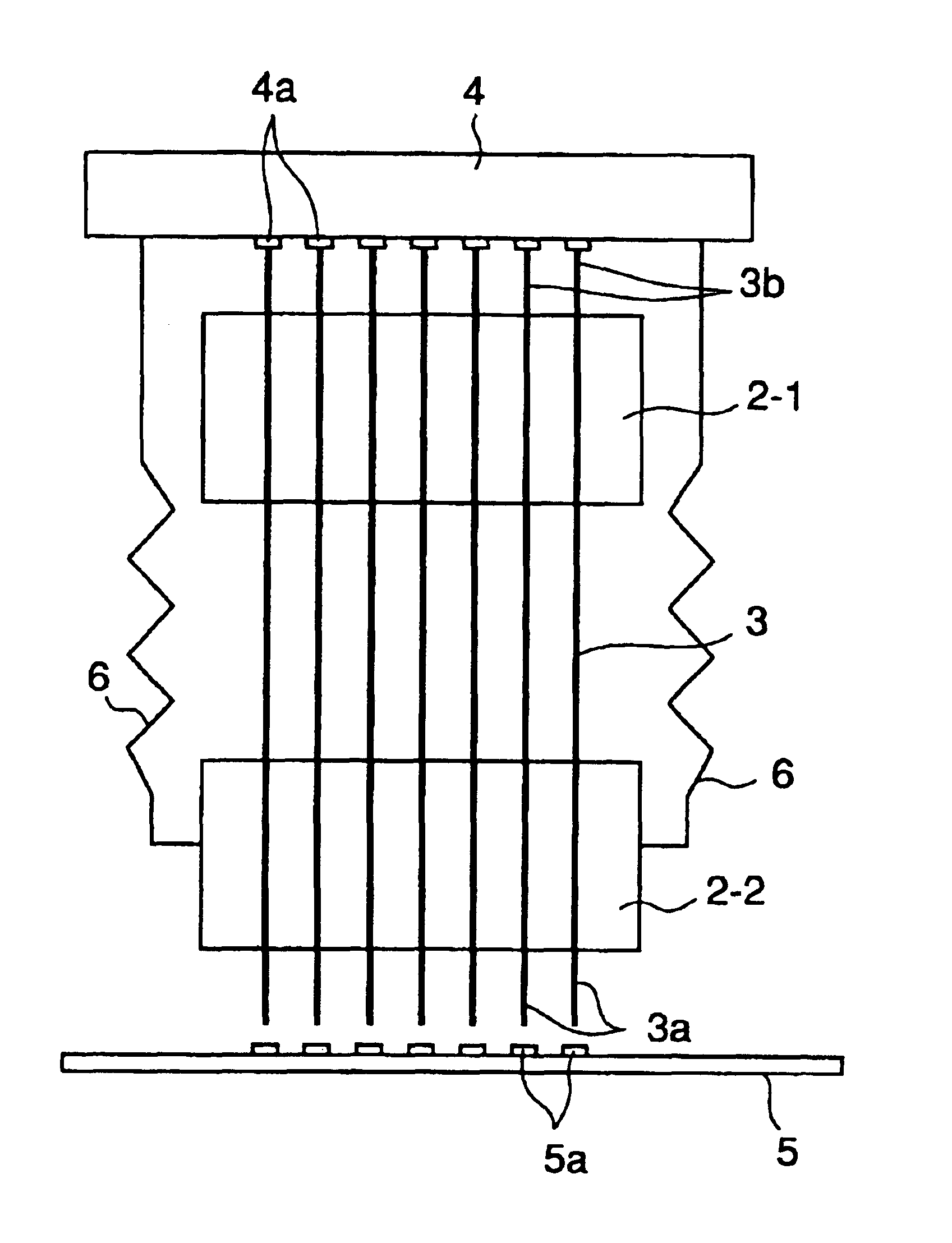
[0099]FIG. 1 is an oblique view of the contactor according to a first embodiment of a present invention.

[0100]As represented in FIG. 1, the contactor of the first embodiment of the present invention is formed of two thin substrates 2-1 and 2-2 and a plurality of wires 3. The substrates 2-1 and 2-2 are thin substrates of an insulating material such as polyimide. The substrates 2-1 and 2-2 are disposed in a spaced manner and the plural wires 3 are provided parallel with each other so as to connect the substrates 2-1 and 2-2.

[0101]The wires 3 are formed of thin lines of a conductive metal such as copper. The wires 3 are capable of causing elastic deformation to some extent. Each of the wires 3 has an end part functioning as a contact terminal 3a and another end part functioning as a contact terminal 3b.

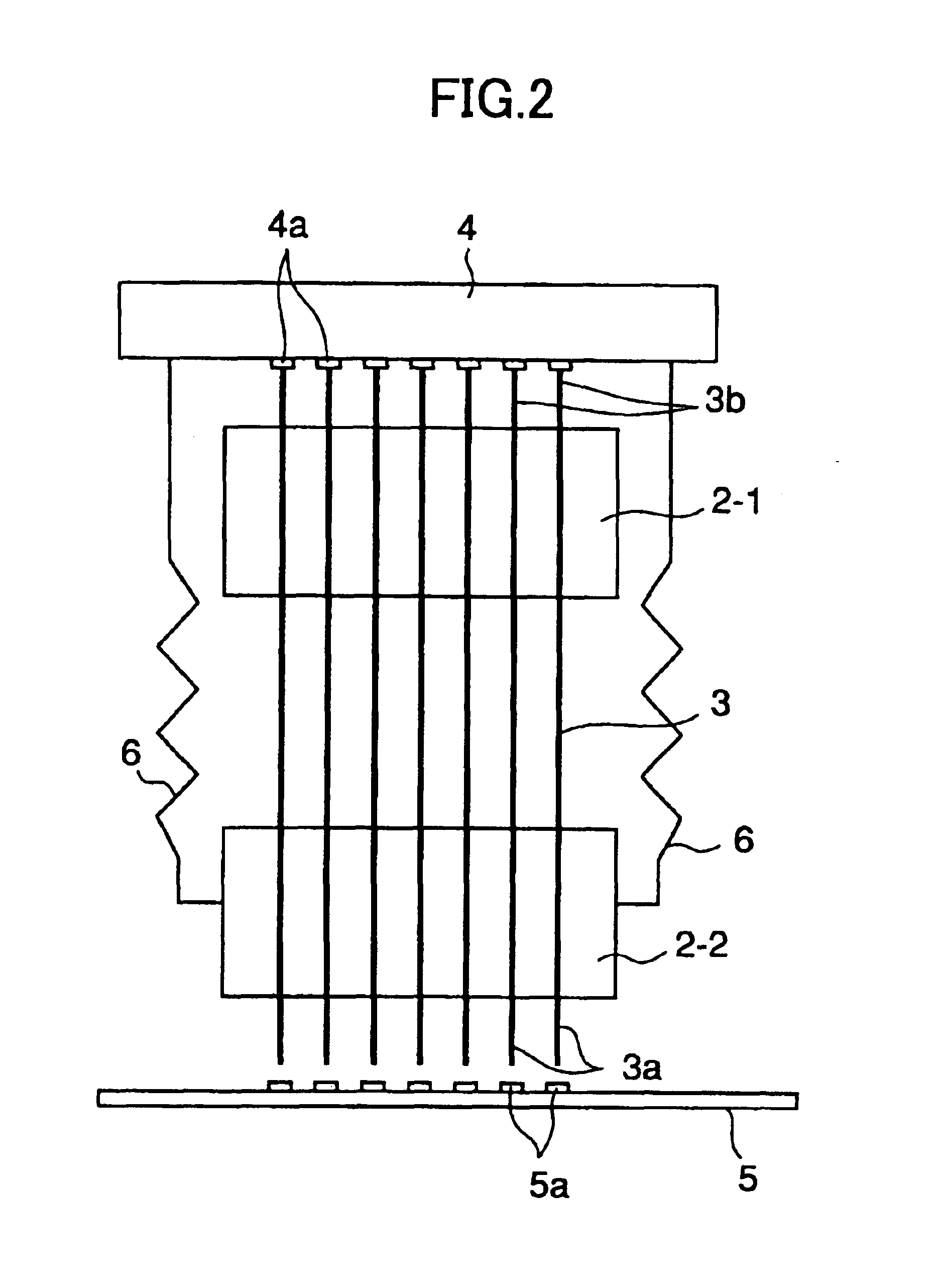
[0102]FIG. 2 is a diagram showing the state for the case the contactor of FIG. 1 is disposed between an electronic component and a probe substrate.

[0103]Referring to F...

second embodiment

(SECOND EMBODIMENT)

[0113]Next, a second embodiment of the present invention will be explained with reference to FIG. 4.

[0114]FIG. 4 is an oblique view diagram of a contactor 11 according to a second embodiment of a present invention.

[0115]Referring to FIG. 4, the contactor 11 also has a construction similar to the abovementioned contactor 1 in that it is attached to the probe substrate 4. Thus, the contactor 11 is provided between the probe substrate 4 and the electronic component 5. The explanation that overlaps with those explained before will be omitted.

[0116]In contactor 11 shown in FIG. 4, it should be noted that the wires 3 are formed on a single substrate 12, while the substrate 12 itself has a construction of causing a deformation. Thus, the wires 3 undergo an elastic extension or contraction in the longitudinal direction thereof together with the substrate 12. In other words, the wires 3 undergo bending together with the deformation of the substrate 12. Preferably, the subs...

third embodiment

(THIRD EMBODIMENT)

[0122]Next, a third embodiment of the present invention will be explained with reference to FIG. 7.

[0123]FIG. 7 is a side view of the contactor according to a third embodiment of the present invention.

[0124]Referring FIG. 7, the contactor 21 of the third embodiment includes a single substrate 22 and plural wires 3 formed on the substrate 22. Further, plural openings 22a are provided in the substrate 21. In the part of the substrate 22 in which the opening 22a is provided, the rigidity of the substrate 223 is decreased, and it becomes possible to curve the substrate 21 easily together with the wires 3. In other words, the spring constant of the contactor 21 is reduced by providing the opening 22a, and the overall the spring constant of the contactor is reduced.

[0125]It should be noted that the opening 22a shown in FIG. 7 is formed near the part of the substrate 22 in which the wires 3 are formed. Thereby, the substrate 22 is left in the part on which the wires 3 are...


PUM


Abstract

A contactor has a film substrate of an insulating material and plural wiring patterns on the substrate. A first end of each wiring pattern extends out from a first edge of the substrate as a first contact terminal and a second end of each wiring pattern extends out from a second edge of the substrate as a second contact terminal, and a part of the contactor located between the first end and second end can be deformed resiliently.

Description

CROSS-REFERENCE TO RELATED APPLICATION[0001]The present application is based on Japanese priority application No. 2002-002744 filed on Jan. 9, 2002, the entire contents of which are hereby incorporated by reference.BACKGROUND OF THE INVENTION[0002]The present invention generally relates to contactors, and especially to a contactor making a contact to electronic components such as a large-scale integrated circuit and a contact process that uses such a contactor.[0003]In recent years, the development of production technology in the field of semiconductor substrate is remarkable. Associated with this, interconnection patterns of large-scale integrated circuits are miniaturized, and along with this, the terminals of large-scale integrated circuits are also miniaturized. Further, the number of the terminals used in an LSI is increasing with remarkable rate.[0004]The demand of miniaturization and high-density mounting is acute especially in the apparatuses that use a large-scale integrate...

Claims


Application Information

Patent Timeline
IPC IPC(8): G01R1/073H01R13/24H01R13/22G01R1/06H01L21/66
CPCG01R1/07314H01R12/714H01R13/24H01R12/52G01R1/06716G01R1/073
Inventor WATANABE, NAOYUKIMARUYAMA, SHIGEYUKITASHIRO, KAZUHIROKOIZUMI, DAISUKEHASHITANI, TAKAFUMI
Owner SOCIONEXT INC
Why Eureka
Try Eureka