
Semiconductor device provided with rewiring layer

a technology of semiconductor devices and rewiring layers, applied in semiconductor devices, semiconductor/solid-state device details, electrical apparatus, etc., can solve the problems of increasing the bonding area of bumps, cracks may be formed in the bonding area, and the reliability of connection of solder bumps, so as to reduce the strain to be generated, increase the bonding area, and reduce the effect of elasticity

Inactive Publication Date: 2005-08-09
INVENSAS CORP
View PDF12 Cites 42 Cited by
  • Summary
  • Abstract
  • Description
  • Claims
  • Application Information

AI Technical Summary

Benefits of technology

[0009]JP-A-6-504408 discloses CSP type semiconductor devices which take a fatigue failure of solder bumps into consideration and are considered as having a high reliability. In this semiconductor device, a sheet-shaped member is attached to the principal surface of a semiconductor element with adhesive which is made of soft and flexible material having a low elasticity ((e.g., elastomer resin: polymer substance having a rubber-like elasticity at an ordinary temperature). Material having an elastic coefficient approximately equal to that of the adhesive is used as a sealing member. Therefore, a coefficient of linear thermal expansion difference between a semiconductor element and a printed circuit board can be absorbed by the adhesive which is made of soft and flexible elastomer resin. Thermal strain applied to a solder bump can therefore be reduced.
[0040]The circumferential area of the bonding area between the bonding pad of the printed circuit board and the external terminal is covered with resin. The strain to be generated in the bonding area is distributed, also, into the interface between the external terminal and resin so that the strain to be generated in the bonding area between the external terminal and bonding pad can be reduced. It is, therefore, possible to reduce a difference between the strains to be generated in the bonding areas on both sides of the package and printed circuit board and to improve the reliability of the semiconductor module as a whole.

Problems solved by technology

A problem associated with CSP having such a structure is a connection reliability of solder bumps.
If such a temperature change is repeated, a crack may be formed in the bonding area.
The crack formed in the bonding area of the bump gradually grows and the bonding area of the bump is ultimately broken.
As the bump of the external terminal is broken, electrical connection between the semiconductor device and an external apparatus via external terminals cannot be maintained.

Method used


Image

  • Semiconductor device provided with rewiring layer
  • Semiconductor device provided with rewiring layer
  • Semiconductor device provided with rewiring layer

Examples


first embodiment

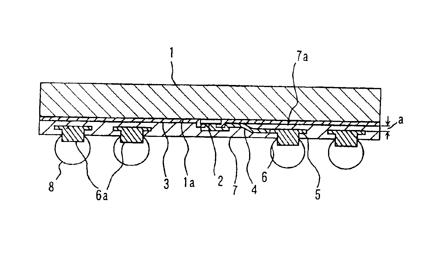
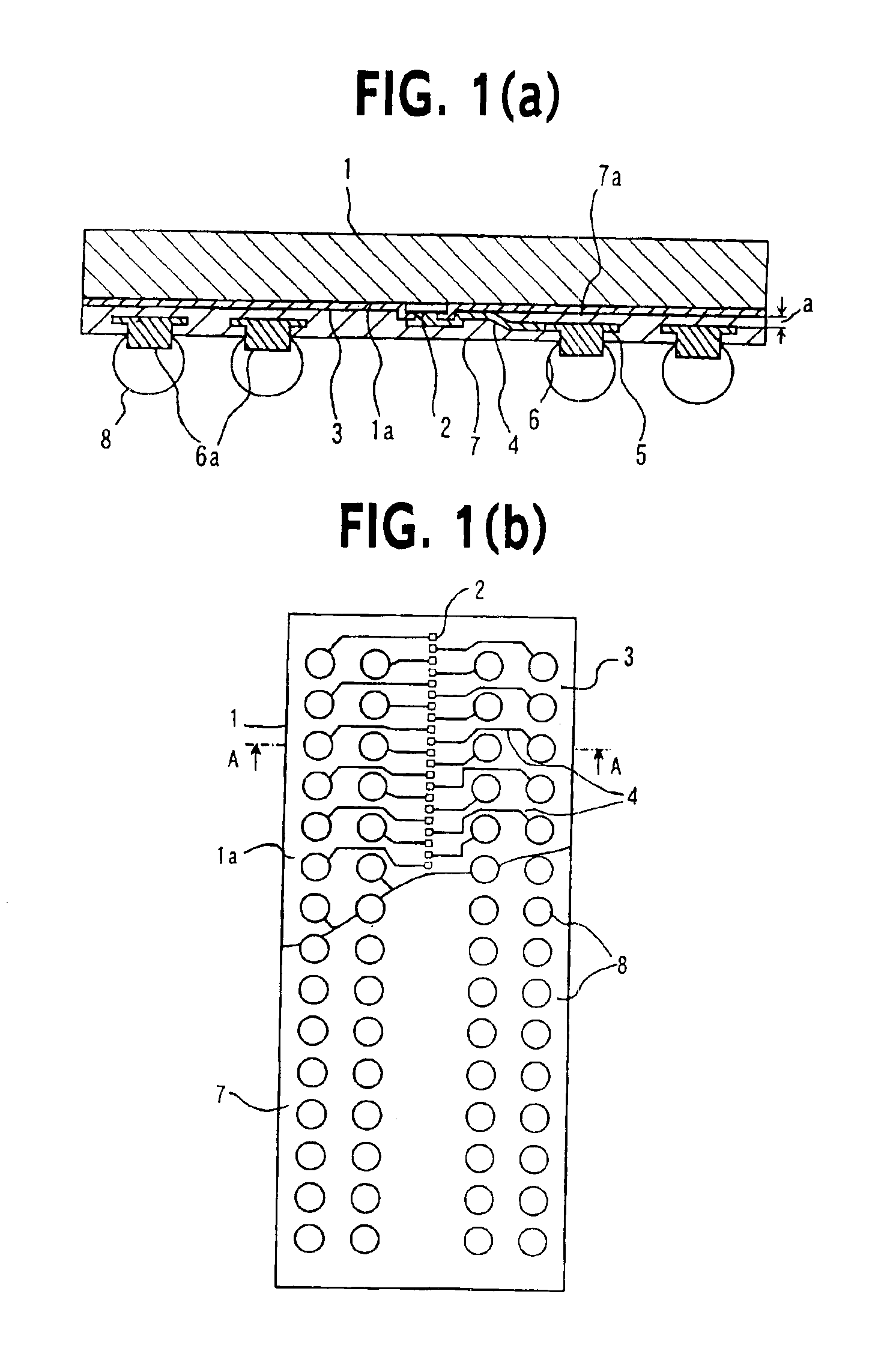
[0059]FIG. 1(a) is a cross sectional view showing a semiconductor device according to the invention. FIG. 1(b) is a plan view of the semiconductor device shown in FIG. 1(a) with a portion of a protective film being removed. The cross sectional view of FIG. 1(a) is a view taken along line A—A shown in FIG. 1(b).

[0060]As shown in FIGS. 1(a) and 1(b), the semiconductor device of the first embodiment of this invention has a semiconductor element 1, a passivation film 3 formed on the surface 1a of the semiconductor element and exposing the surfaces of each pad 2, a conductive wiring line 4 connected to each pad 2, a land 5 connected to each conductive wiring line 4, a protective film 7, a projection 6 formed on each land 5, and external terminals 8.

[0061]The pads 2 are disposed vertically in the central area of the surface 1a of the semiconductor element. The conductive wiring line 4 connected to each pad 2 extends to the land 5 on the semiconductor element surface 1a on which the projec...

second embodiment

[0090]FIG. 5 is a cross sectional view of a semiconductor device according to the invention.

[0091]The fundamental structure of the semiconductor device of the second embodiment of the invention shown in FIG. 5 is similar to the first embodiment shown in FIG. 1. A different point from the first embodiment resides in that a portion 6b of a projection 6 surrounded by a protective film 7 is narrower than a protruded portion 6a to be bonded to an external terminal 8 so that an intervening portion 7c of the protective film 7 exists in a projected area of the protruded portion 6a of the projection 6.

[0092]According to the semiconductor device of the second embodiment of the invention, the intervening portion 7c of the protective film 7 exists in a projected area of the protruded portion 6a of the projection 6. Therefore, deformation of the external terminal 8 to be caused by a coefficient of linear thermal expansion difference between the semiconductor device and printed circuit board can ...

third embodiment

[0096]FIG. 7 is a cross sectional view showing a semiconductor device according to the invention.

[0097]As shown in FIG. 7, the semiconductor device of the third embodiment of this invention has a semiconductor element 1, a passivation film 3 formed on the surface 1a of the semiconductor element and exposing the surfaces of each pad 2, a conductive wiring line 4 connected to each pad 2, a land 5 connected to each conductive wiring line 4, first and second protective films 7 and 15, and external terminals 8.

[0098]The pads 2 are disposed vertically in the central area of the surface 1a of the semiconductor element. The conductive wiring line 4 connected to each pad 2 is constituted of a first conductive wiring line 4a disposed on the semiconductor element surface 1a and a second conductive wiring line 4b connected to the land 5. The first protective film 7 is formed over the semiconductor element surface 1a, covering the passivation film 3 and first conductive wiring line 4a and a port...


PUM


Abstract

In a small semiconductor device having external terminals on a semiconductor element and a semiconductor module mounted with the small semiconductor device, disconnection of the external terminals is prevented when a temperature change occurs under the conditions that the semiconductor device is mounted on a printed circuit board. To achieve this a projection is formed on a land which is an external terminal bonding area of the semiconductor device, and a protruded portion of the projection is bonded to the external terminal. An intervening portion of a protective film made of resin material is formed between the lands and semiconductor element.

Description

TECHNICAL FIELD[0001]The present invention relates to a small semiconductor device having external terminals on a semiconductor element, and, more particularly, to a small semiconductor device having a semiconductor element with various functions manufactured by wafer processes and to a semiconductor module having a semiconductor device with external terminals mounted on a printed circuit board.BACKGROUND ART[0002]Flip chip bonding has been conventionally used as high density mount technology for mounting a semiconductor element on a printed circuit board or the like without packaging it. With this flip chip bonding technology, external terminals are formed on pads of a semiconductor element, and the pads of the semiconductor element and bonding pads on a printed circuit board are electrically and mechanically connected via the external terminals.[0003]With flip chip bonding, however, the layout and size of external terminals are restricted by the layout and size of pads of a semico...

Claims


Application Information

Patent Timeline
IPC IPC(8): H01L23/28H01L23/31H01L21/60H01L23/485H01L23/12
CPCH01L23/3114H01L24/10H01L24/13H01L2924/0002H01L2224/13099H01L2924/01004H01L2924/01013H01L2924/01029H01L2924/01078H01L2924/01079H01L2924/01082H01L2924/01322H01L2924/30105H01L2224/05541H01L2224/05548H01L2924/01005H01L2924/01006H01L2924/01019H01L2924/01024H01L2924/01033H01L2924/01047H01L2924/01087H01L2924/014H01L2224/13006H01L2224/05572H01L2224/0401H01L2924/207H01L2924/00H01L2224/05552H01L2224/13H01L2224/05124H01L2224/05139H01L2224/05147H01L2224/05155H01L2224/05171H01L2224/05644H01L2224/05655H01L2224/05144H01L2924/0001H01L2224/0615H01L2224/05569H01L2224/13024H01L24/05H01L24/03H01L24/02H01L2224/023H01L2924/00014H01L2224/02H01L2924/013H01L23/48
Inventor YAGUCHI, AKIHIROMIURA, HIDEOKAZAMA, ATSUSHINISHIMURA, ASAO
Owner INVENSAS CORP
Learn More