Under bump metallization structure of a semiconductor wafer

a technology of bump metallization and semiconductor wafer, which is applied in the direction of semiconductor devices, semiconductor/solid-state device details, electrical devices, etc., to achieve the effect of enhancing the bonding strength of the bump and slowing down the formation of inter-metallic compounds

Active Publication Date: 2005-08-16
ADVANCED SEMICON ENG INC
View PDF2 Cites 26 Cited by
  • Summary
  • Abstract
  • Description
  • Claims
  • Application Information

AI Technical Summary

Benefits of technology

[0010]In view of the above-mentioned problems, an objective of this invention is to provide an under bump metallization structure formed between the bonding pads and the solder bumps to slow down the formation of inter-metallic compound, i.e. discontinuous blocks, in the barrier layer so as to enhance the bonding strength of the bumps to the bonding pads and the reliability of said bumped wafer or bumped chips.
[0011]To achieve these and other advantages and in accordance with the purpose of the invention, as embodied and broadly described herein, the invention provides an under bump metallization structure disposed between bonding pads and solder bumps which comprises tin. Therein, the under bump metallization structure at least comprises an adhesive layer disposed on the bonding pads, a first barrier layer formed on the adhesive layer, a wetting layer disposed on the first barrier layer, and a second barrier formed on the wetting layer. It should be noted that the second barrier layer can slow down the formation of the inter-metallic compound in the interface between the first barrier layer and the wetting layer due to the material of the second barrier layer mainly comprising lead and tin so as to prevent discontinuous blocks, i.e. Ni3Sn4, from being formed in the first barrier layer of the under bump metallization structure. In such a manner, it will prevent the solder bumps from peeling off from the under bump metallization structure.

Problems solved by technology

However, lead is a hazard and poisoned material so lead-free alloy becomes the mainstream material of the solder bump 108.

Method used


Image

  • Under bump metallization structure of a semiconductor wafer
  • Under bump metallization structure of a semiconductor wafer
  • Under bump metallization structure of a semiconductor wafer

Examples


second embodiment

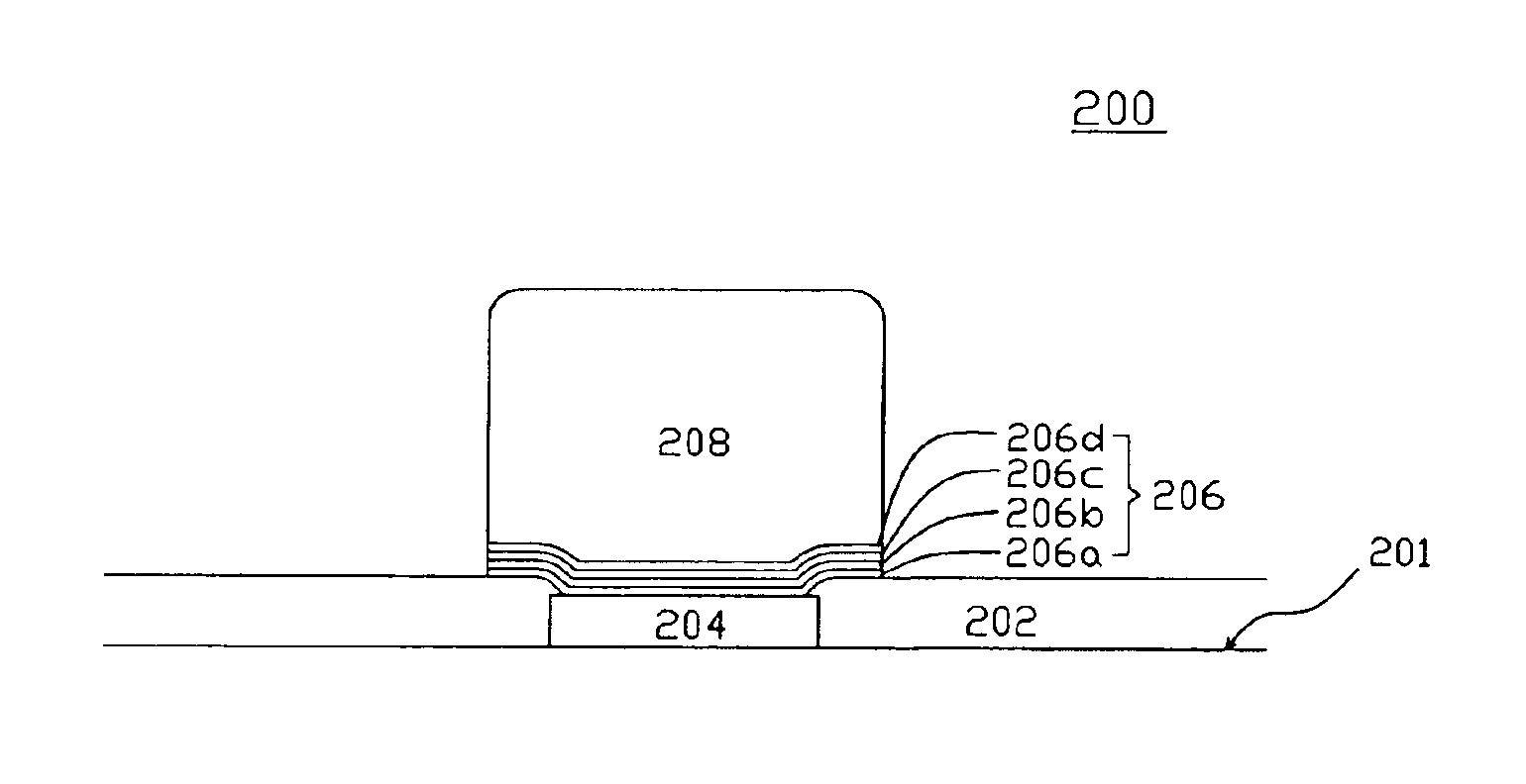
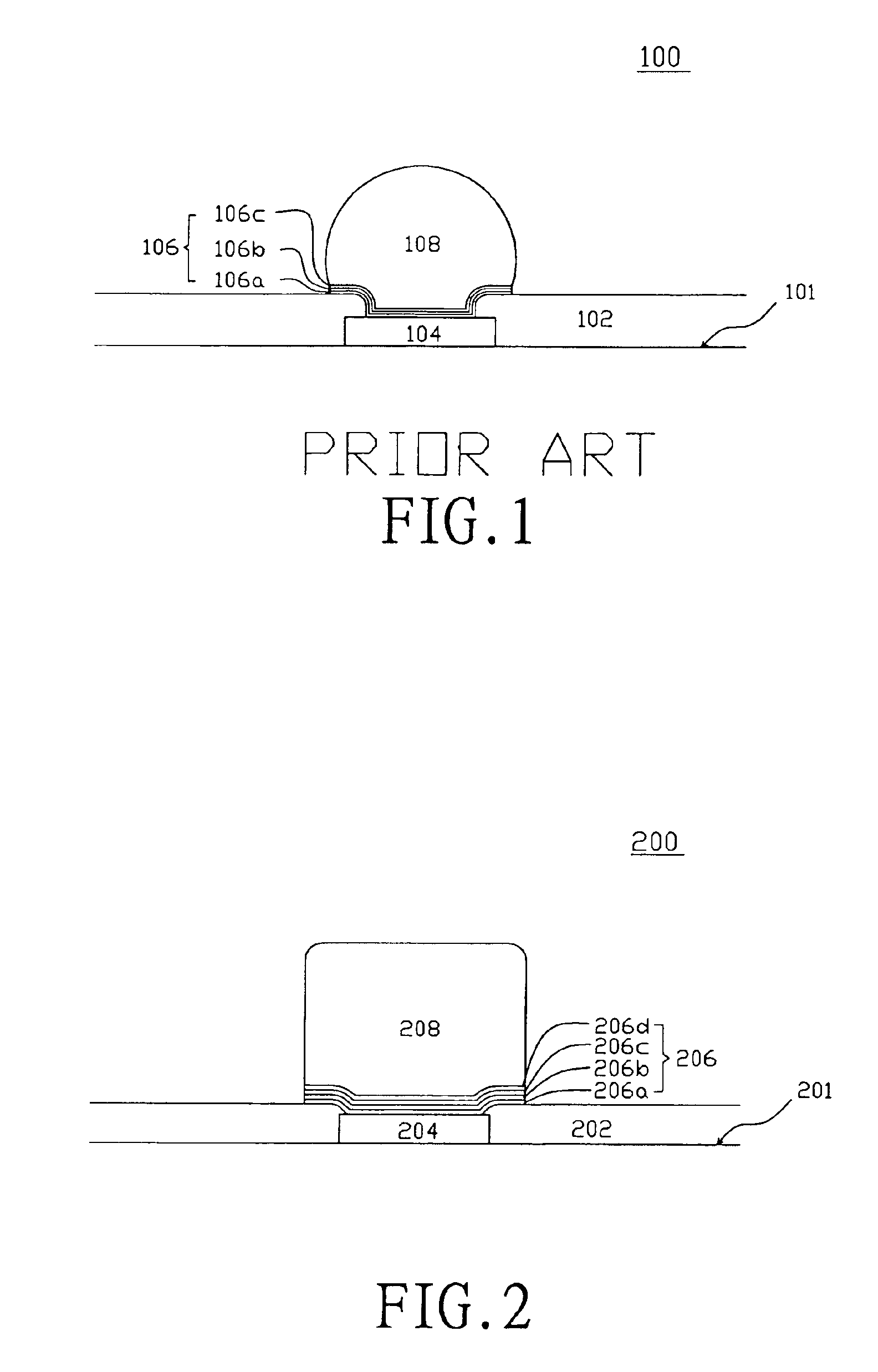
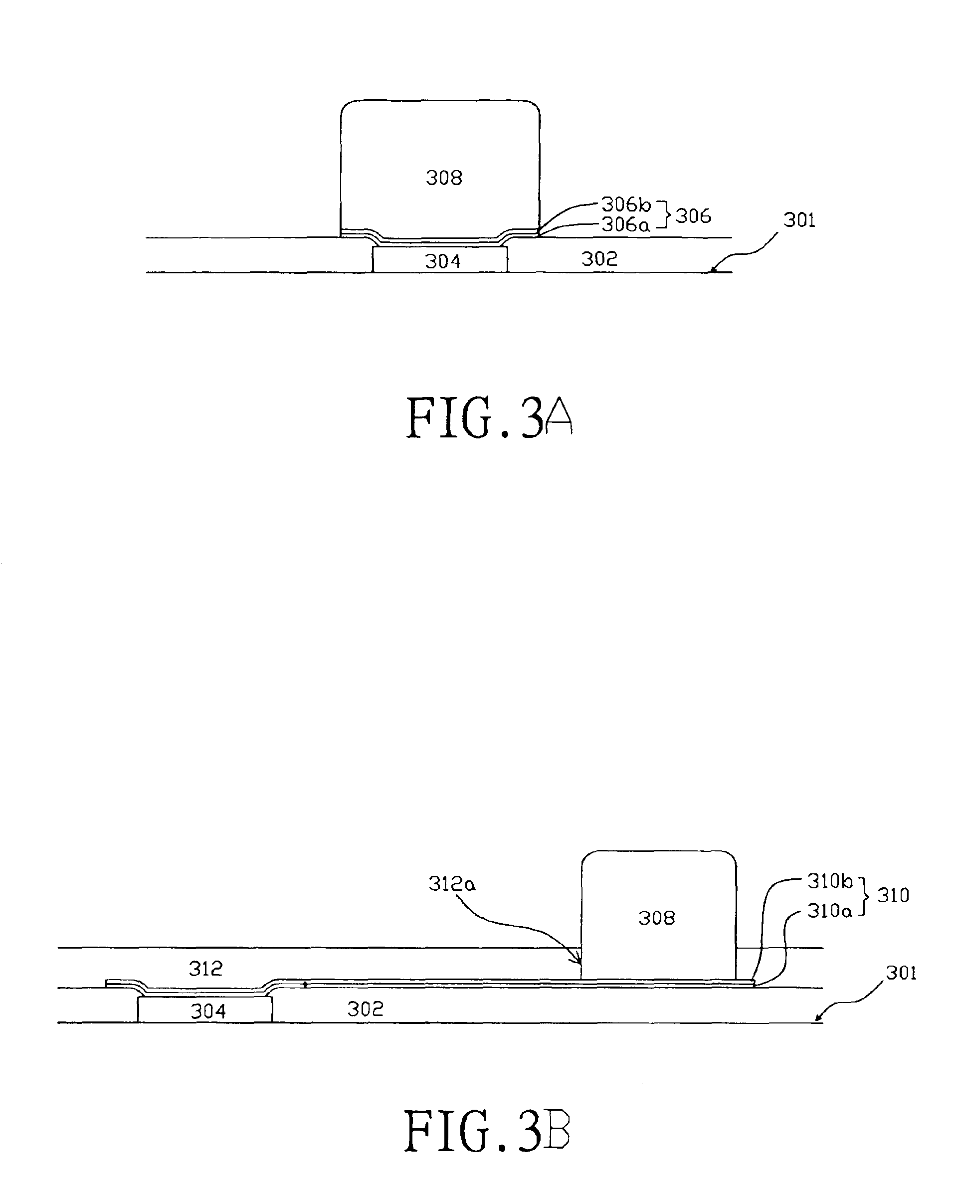
[0025]Moreover, a second preferred embodiment is provided as shown in FIG. 3A. Therein, the under bump metallization structure 306 of this invention may comprise two electrically conductive layers 306a and 306b. A first electrically conductive layer 306a at least comprises nickel and a second electrically conductive layer 306b mainly comprises lead wherein the first electrically conductive layer 306a is directly formed on the bonding pads 304 and the second electrically conductive layer 306b is directly connected to the bumps 308.

third embodiment

[0026]Furthermore, per mentioned above, when the under bump metallization structure is extended over the active surface 301 of the semiconductor wafer 300 to be taken as this invention, said under bump metallization structure are taken as a redistributed structure 310 (as shown in FIG. 3B). It should be noted that a portion of the redistributed structure 310 is exposed out of the passivation layer 312 through the opening 312a to be regarded as a redistributed pad and the upper layer of the redistributed pad is mainly made of lead or high-lead solder. Therein, the redistributed structure 310 comprises a first electrically conductive layer 310a and a second electrically conductive layer 310b for connecting the bumps 308, and the passivation layer 312 may be formed of a polymer material, such as polyimide and Benzocyclobutence (BCB).


PUM


Abstract

An under bump metallurgy structure is applicable to be disposed above the wafer and on the bonding pads of the wafer. The wafer comprises a passivation layer and an under bump metallurgy structure. The passivation layer exposes the wafer pads, and the under bump metallurgy structure including an adhesive layer, a first barrier layer, a wetting layer and a second barrier layer are sequentially formed on the bonding pads. Specifically, the material of the second barrier mainly includes lead.

Description

BACKGROUND OF THE INVENTION[0001]1. Field of Invention[0002]This invention relates to an under bump metallization structure of a semiconductor wafer. More particularly, the present invention is related to an under bump metallization structure of a wafer for enhancing the mechanical strength of the connection of the bonding pads to the wafer and the solder bumps.[0003]2. Related Art[0004]In this information explosion age, integrated circuit products are used almost everywhere in our daily life. As fabricating technique continue to improve, electronic products having powerful functions, personalized performance and a higher degree of complexity are produced. Nowadays, most electronic products are relatively light and have a compact body. Hence, in semiconductor production, various types of high-density semiconductor packages, for example ball grid array package (BGA), chip-scale package (CSP), multi-chips module package (MCM) and flip chip package (F / C), have been developed.[0005]Howe...

Claims


Application Information

Patent Timeline
Patent Type & Authority Patents(United States)
IPC IPC(8): H01L21/02H01L21/60H01L23/485H01L23/48
CPCH01L24/11H01L24/13H01L2224/13099H01L2924/01013H01L2924/01022H01L2924/01029H01L2924/01074H01L2924/01078H01L2924/01082H01L2924/14H01L2924/01006H01L2924/01023H01L2924/01024H01L2924/01033H01L2924/014H01L2224/131H01L2924/0001H01L2224/05027H01L2224/05022H01L2224/0508H01L2224/05001H01L2224/05572H01L2224/05184H01L24/05H01L2224/023H01L2224/05647H01L2924/00014H01L2224/05124H01L2224/05147H01L2224/05155H01L2224/05166H01L2224/05171
Inventor HUANG, MIN-LUNG
Owner ADVANCED SEMICON ENG INC
Why Eureka
Try Eureka