LDMOS with guard ring (of same type as drain) surrounding the drain

a technology of guard rings and drains, applied in semiconductor devices, diodes, electrical devices, etc., to achieve the effect of higher doping concentration

a technology of guard rings and drains, applied in semiconductor devices, diodes, electrical devices, etc., to achieve the effect of higher doping concentration

US6933559B1Inactive Publication Date: 2005-08-23US PHILIPS CORP +1

Image

  • LDMOS with guard ring (of same type as drain) surrounding the drain
  • LDMOS with guard ring (of same type as drain) surrounding the drain
  • LDMOS with guard ring (of same type as drain) surrounding the drain

Examples


Embodiment Construction

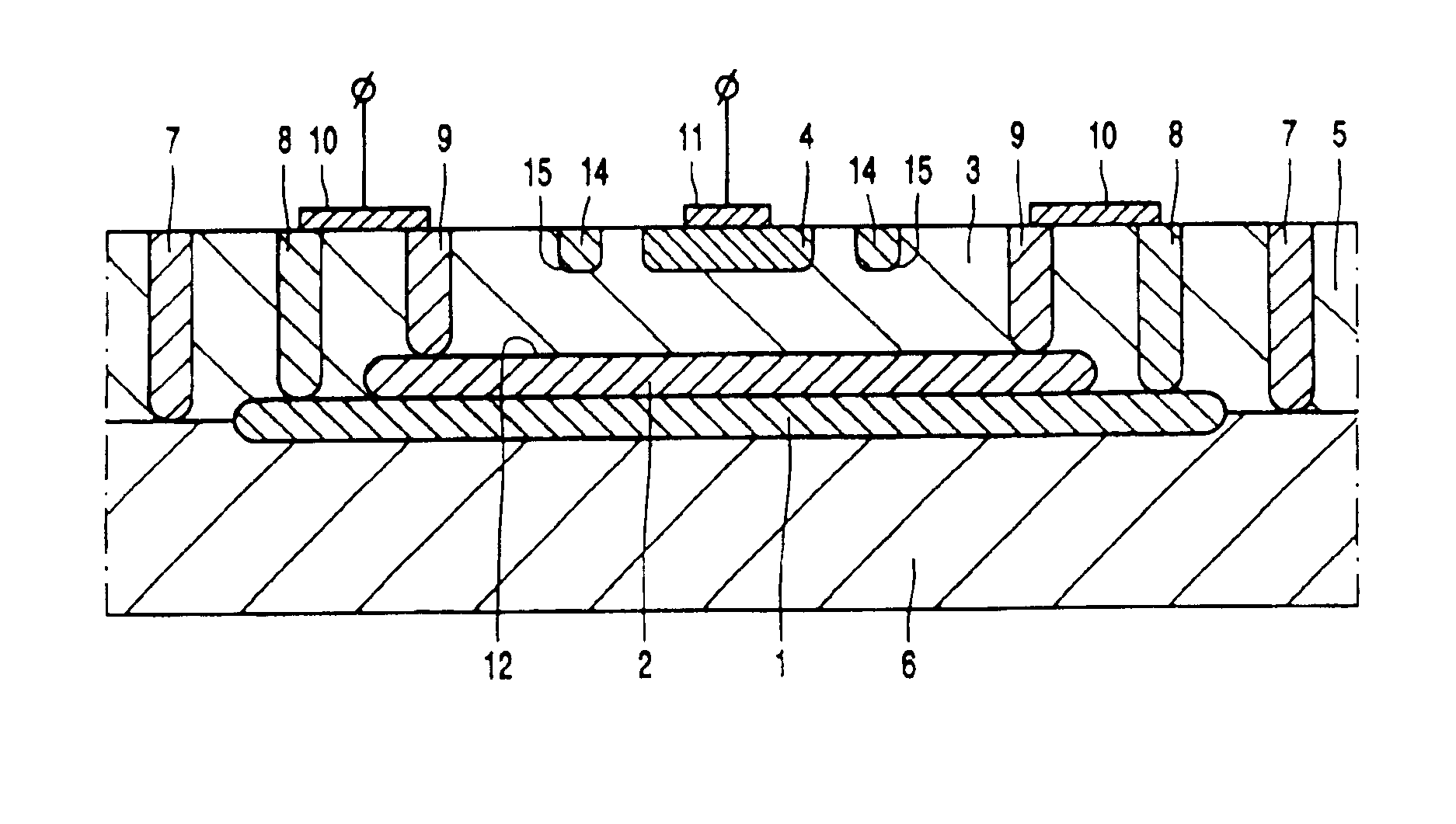
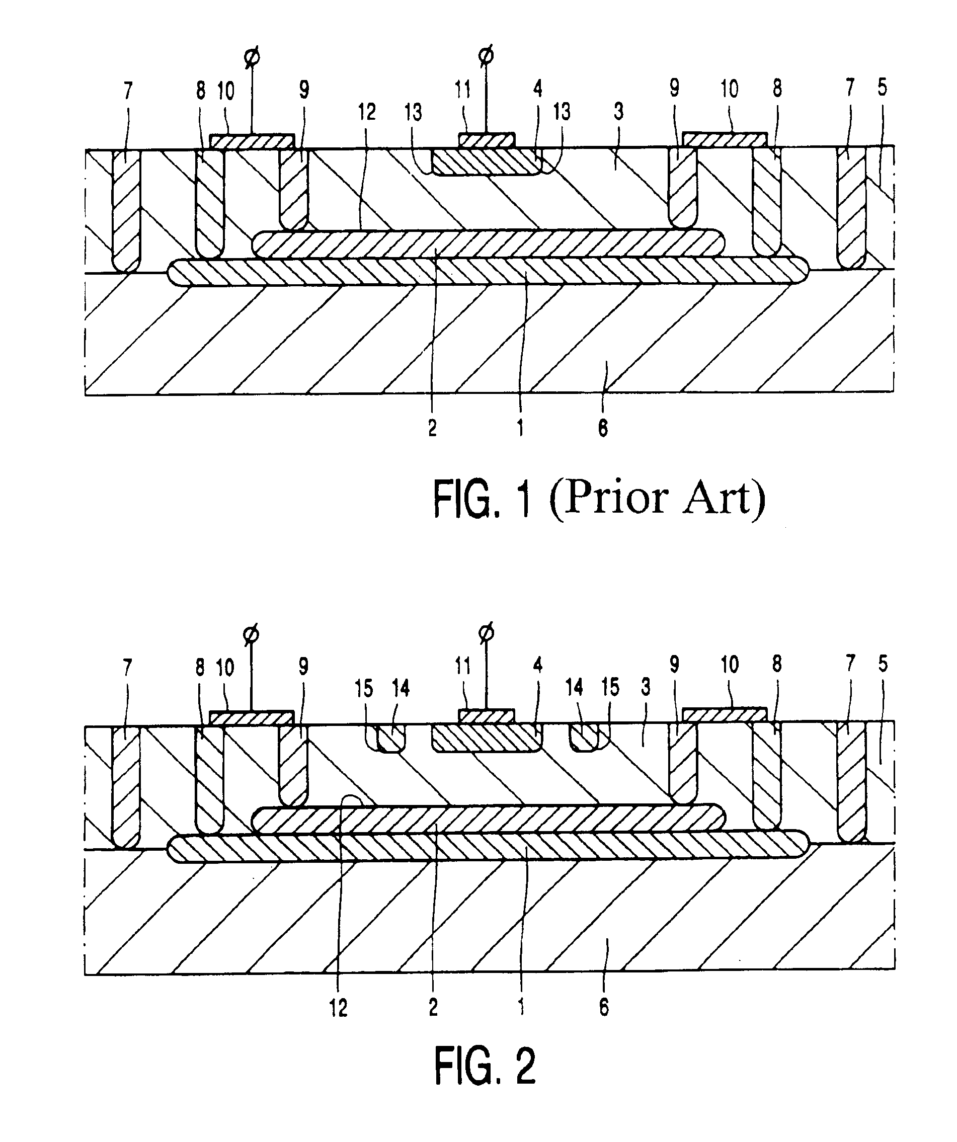
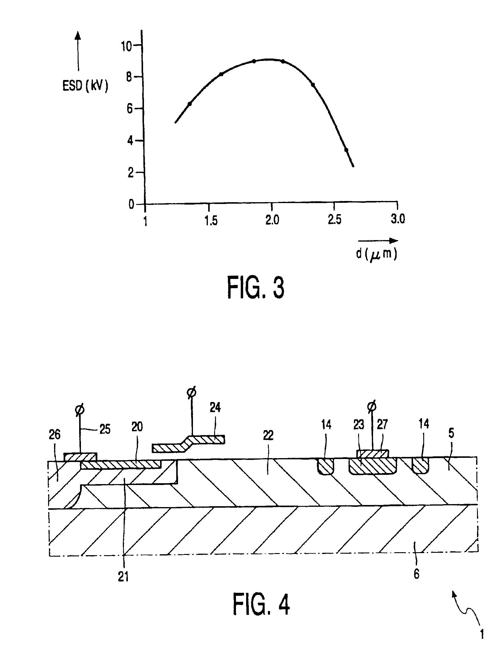
[0011]It is to be noted that the drawings are only diagrammatic and not to scale. Hereinbelow, the invention will be described by means of a diode which can suitably be used, for example, as a protection diode against ESD in an integrated circuit. To illustrate the invention, FIG. 1 shows a known diode and FIG. 2 shows an embodiment of such a diode in accordance with the invention. The device comprises a semiconductor body provided with: a first region 1 of a first conductivity type, in this example the n-type, a second region of the second, opposite conductivity type, i.e. in this example the p-type, which adjoins the first region 1, a third region 3 of the n-type adjoining the second region 2 and separated from the first region 1 by the second region, and a fourth region 4 of the n-type adjoining the third region 3, which fourth region forms a contact zone and has a higher doping concentration than the third region 3. The region 3 is formed by an island-shaped part of an n-type ep...


PUM


Abstract

In high-voltage devices comprising a lightly doped region (3) provided with a heavily doped contact zone 4, damage caused by local breakdown at the corner of the contact zone may occur as a result of the Kirk effect at a high current density. To improve the robustness of the device, an annular protection zone (14) of the same conductivity type is provided so as to surround the contact zone at a small distance. As a result, breakdown will occur initially at the corner of the protection zone. However, due to the resistance between the protection zone and the contact zone, a more uniform current distribution is obtained, which prevents damage caused by local current concentration.

Description

BACKGROUND OF THE INVENTION[0001]The invention relates to a semiconductor device comprising a semiconductor body having a first region of a first conductivity type and, adjacent thereto, a second region of the second, opposite, conductivity type, a third region of the first conductivity type, which is adjacent the second region and separated from the first region by the second region, and a fourth region of the first conductivity type which is separated from the second region by the third region and which has a higher doping concentration than the third region, the first, the second and the fourth region each being provided with a terminal. Said fourth region may be considered to be a contact zone of the third region of the same conductivity type. Consequently, the succession of various regions described herein forms a horizontal or a vertical npn or pnp structure which can suitably be used, for example, as a transistor (bipolar or MOS) or as a diode.[0002]It has been found that, in...

Claims


Application Information

Patent Timeline
23 Aug 2005
Publication
US6933559B1
IPC
H01L29/06; H01L29/78; H01L29/02; H01L27/02; H01L29/66; H01L29/861; H01L29/08; H01L29/10; H01L29/423; H01L29/40; H01L27/04; H01L21/822
CPC
H01L27/0255; H01L29/0626; H01L29/0878; H01L29/7816; H01L29/861; H01L29/8611; H01L29/42368; H01L29/78
Inventors
VAN ROIJEN, RAYMOND; EGBERS, JOHANNES HENDRIK HERMANUS ALEXIUS